Explore our advanced catalog of processing units, memory models, motherboard architectures, and custom thermal solutions integrated into CE Certified Multilayer PCBs.
In the contemporary hardware landscape, the exponential rise of Artificial Intelligence (AI), Machine Learning (ML), and high-frequency communication protocols has fundamentally transformed printed circuit board design requirements. Multi-layer printed circuit boards (PCBs) act as the central circulatory system of high-density computers, server arrays, and networking systems. As systems shift from traditional double-sided architectures to advanced multi-layer stackups (frequently exceeding 8, 12, or even 24 layers), maintaining pristine signal integrity while adhering to rigorous regulatory guidelines is paramount.
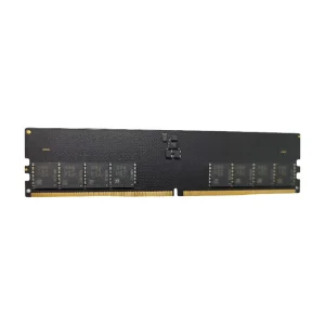
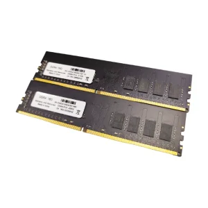
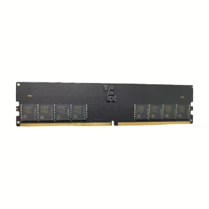
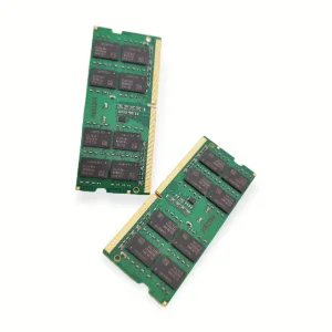
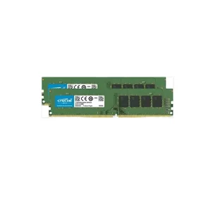
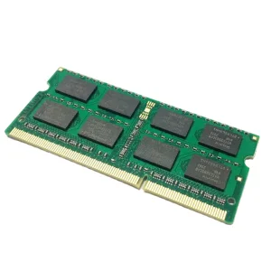
A high-speed multilayer PCB is far more than an array of laminated copper traces; it is a complex electro-magnetic waveguide system. In designs containing dense component integration, such as DDR5 RAM interfaces operating at frequencies exceeding 5600MHz to 6000MHz, minor discrepancies in copper roughness, dielectric constant (Dk) deviation, or lamination consistency will result in devastating signal degradation, electromagnetic interference (EMI), and hardware failure. Partnering with a vetted, CE Certified Multilayer PCBs Factory ensures the implementation of precise fabrication tolerances, strict material sourcing, and complete adherence to global safety and compatibility frameworks.
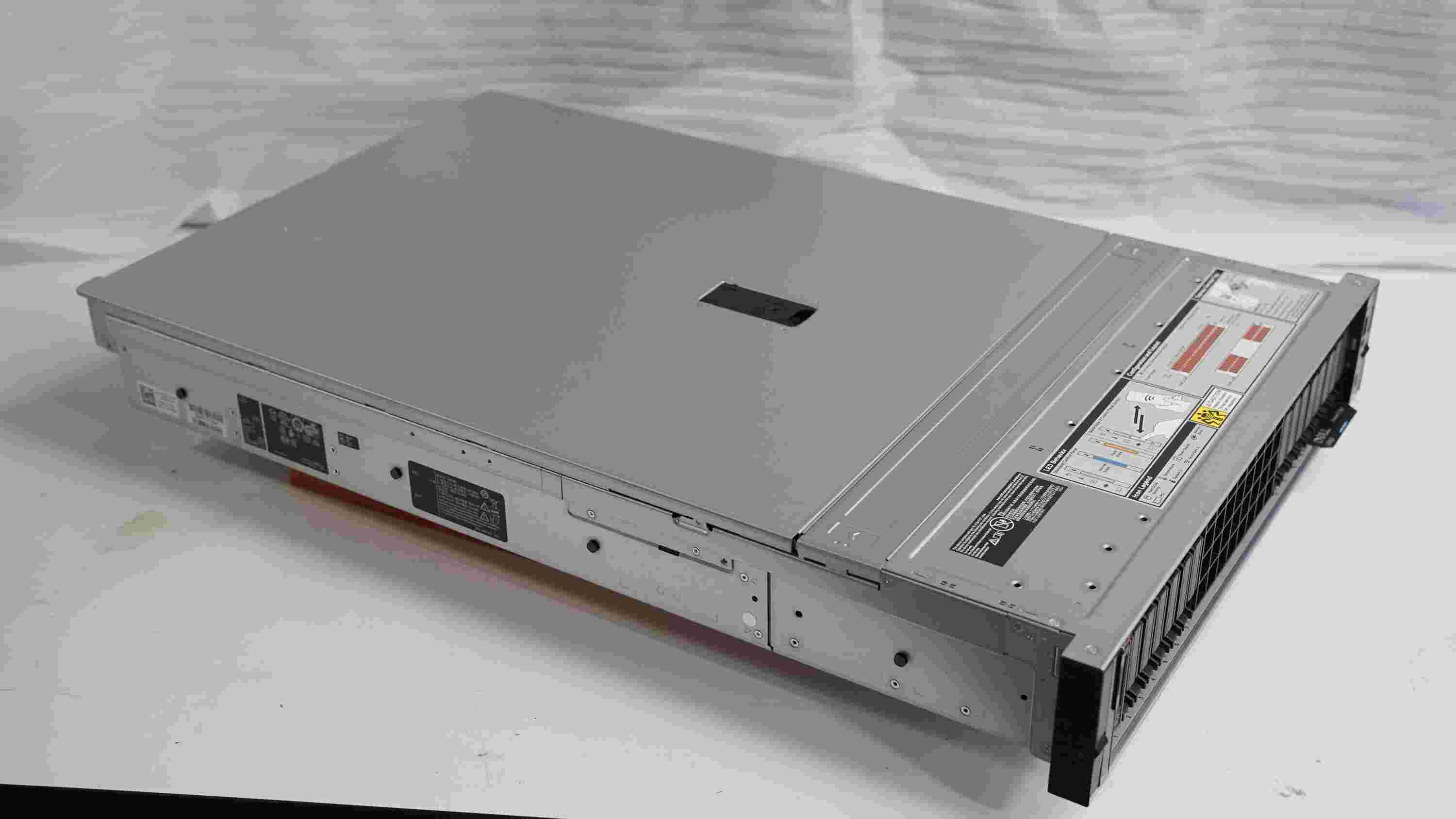
To understand how advanced PCB stackups integrate with next-generation memory and processing architectures, we examine our partner facility, VoltDRAM Semiconductor Co., Ltd. Established between 2015–2018, VoltDRAM has emerged as a premier developer of high-speed memory systems and advanced layout engineering, showcasing a robust production footprint tailored for modern enterprise applications.
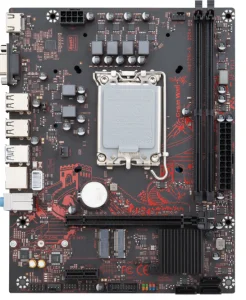
Operating with a highly specialized manufacturing area of approximately 320–480㎡, VoltDRAM operates with an international trade focus, primarily serving critical technology corridors across North America, Europe, Southeast Asia, and the Middle East. Maintaining a vast ecosystem of over 600–1,500 supply chain partners allows the execution of specialized product updates, delivering approximately 120–450 new product variants yearly. This agile manufacturing and R&D architecture directly supports custom motherboard and high-frequency memory designs.
From controlled impedance pathways to thermal management, modern multilayer circuit boards must navigate dense constraints.
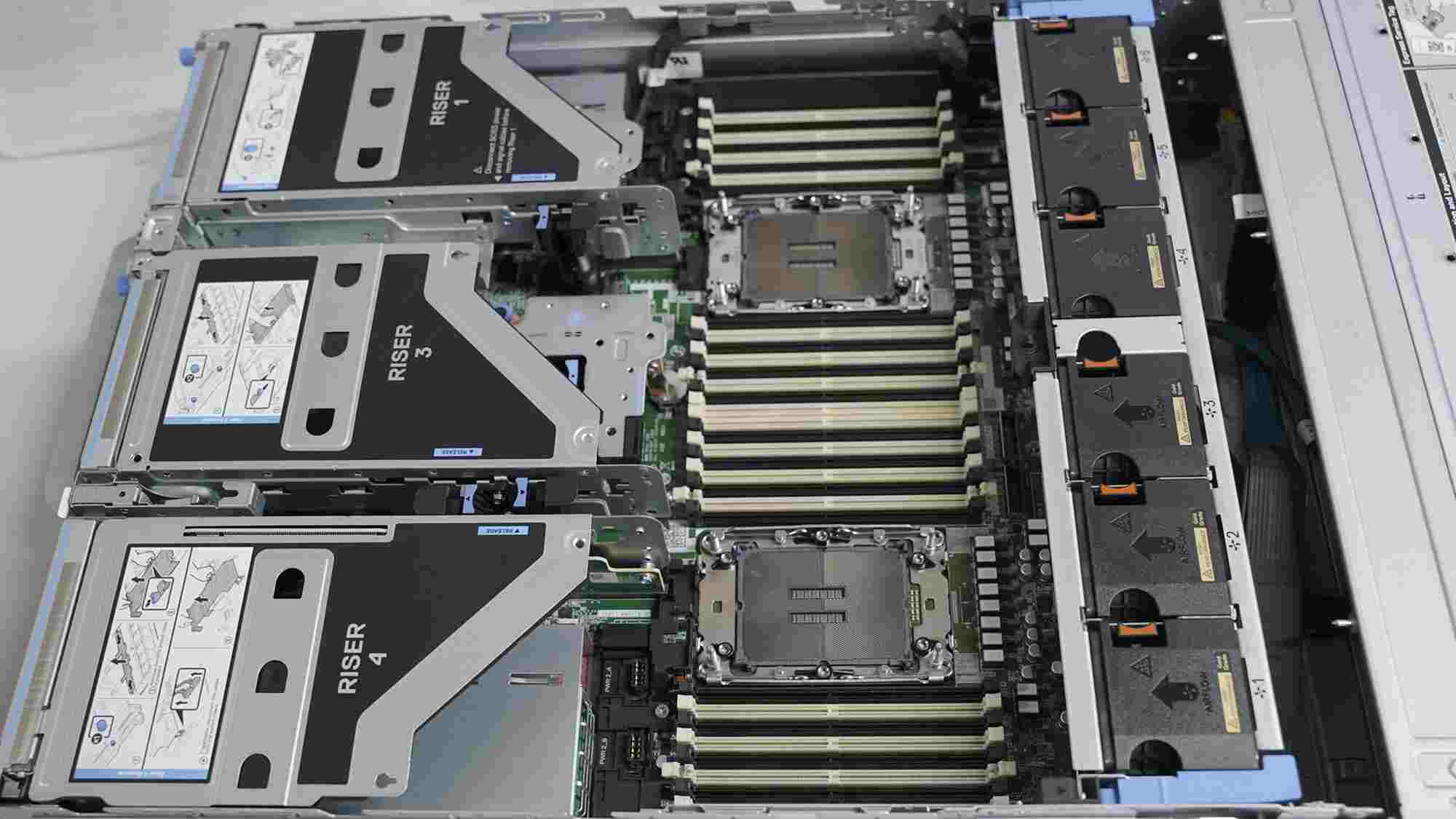
Maintaining signal trace geometry is critical for DDR5 speeds. Path configurations utilize microstrips, embedded microstrips, and striplines configured to minimize attenuation and keep differential impedance within a 5% margin.
Using premium prepregs and core materials with Low-Dissipation (low Df) factors ensures minimum signal degradation across multi-layered stackups, especially under variable thermal conditions.
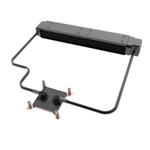
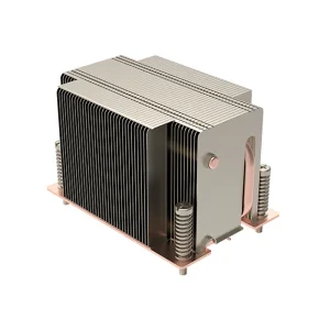
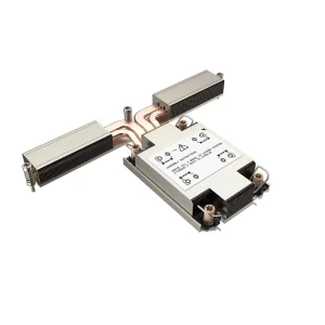
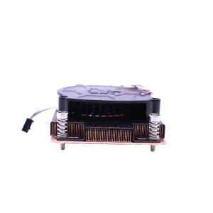
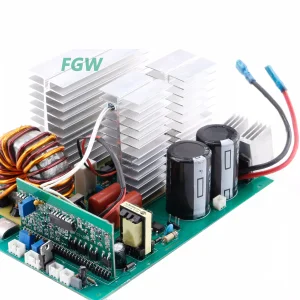
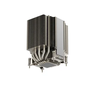
Integrating complex heavy copper power planes and thermal vias prevents hotspots. Crucial for high-performance server motherboard architectures operating under intense, continuous computing loads.
To market hardware globally, compliance with European safety and performance criteria is a crucial milestone. CE Certification encompasses several technical directives that multilayer PCBs must satisfy during design and manufacturing.
The Electromagnetic Compatibility (EMC) directive dictates that electronic systems must not emit electromagnetic noise that compromises adjacent hardware, and they must resist external interference. Multilayer PCBs facilitate compliance through:
The Restriction of Hazardous Substances (RoHS) requires PCBs to be lead-free (Pb-free). Factories must implement high-temperature assembly processes because lead-free solders (e.g., SAC305) require higher melting points. Consequently, substrate material must resist thermal shock without delamination during soldering cycles.
For PCBs handling high-voltage paths, the Low Voltage Directive requires specific spacing parameters:
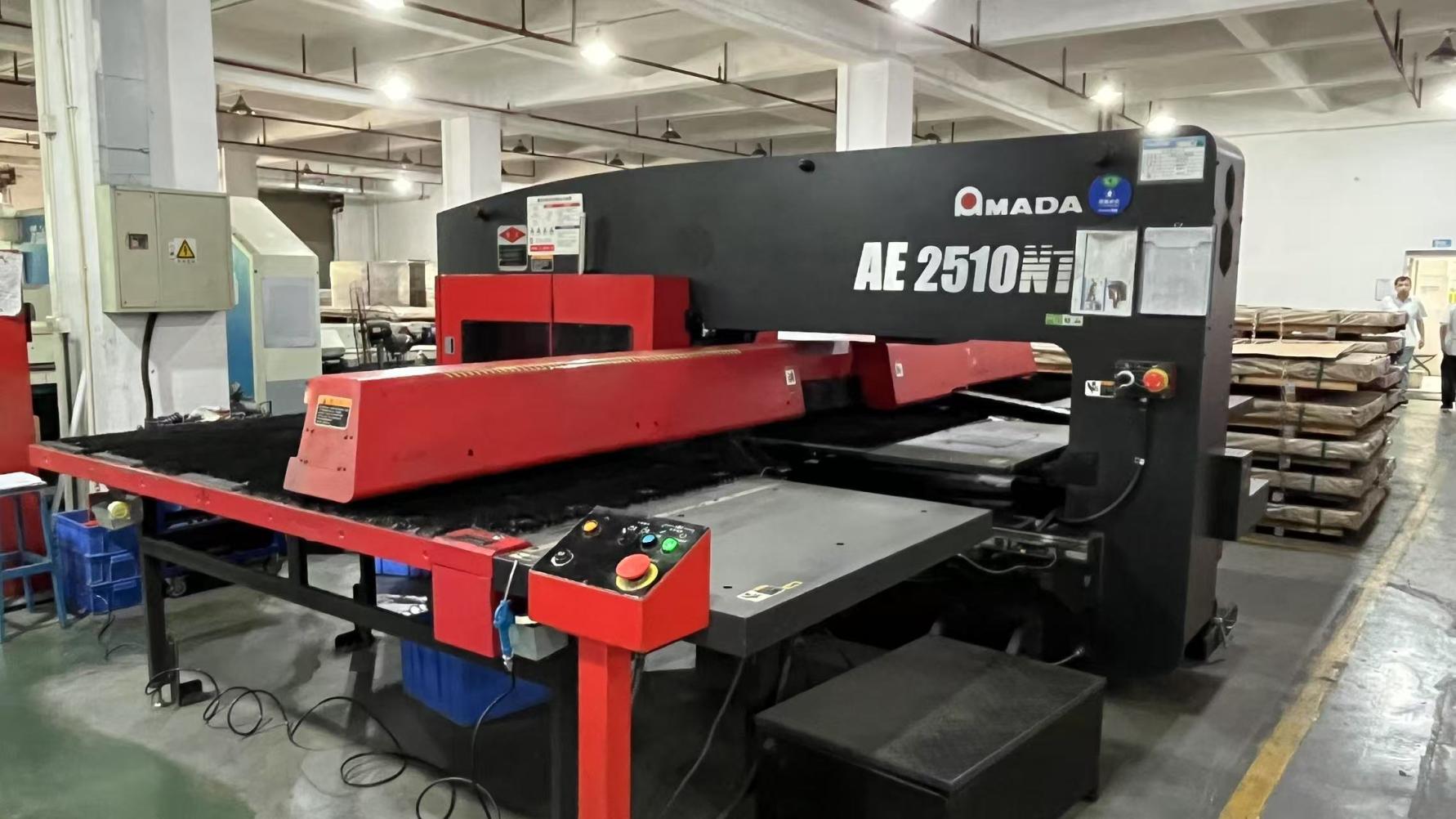
For modern computing systems, raw materials must undergo rigorous verification before assembly. Our manufacturing partner, VoltDRAM, implements multi-layered inspection systems:
As memory interfaces transition to DDR6 and processors demand higher current densities, multilayer PCBs face new challenges. Ultra-low-loss copper foils (like HVLP) and substrate-like layouts (SLP) are becoming standard to limit skin-effect losses. Research focuses on embedding optical waveguides within FR4 layers, paving the way for hybrid electro-optical processing systems.
Answers to common design and regulatory compliance questions regarding multilayer PCB systems.
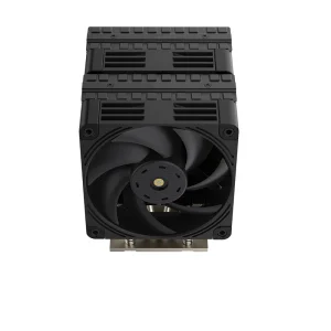
Integrating these advanced designs requires high-quality memory interfaces and cooling solutions for enterprise equipment.

A visual overview of our advanced production floors, testing chambers, and semiconductor development laboratories.