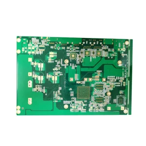
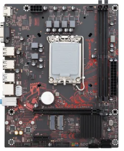
In modern electronic design, the demand for higher bandwidth, reduced component footprints, and complex signal integrity has accelerated the transition from simple double-sided boards to sophisticated multi-layer printed circuit boards (PCBs). A multi-layer PCB consists of three or more conductive copper layers laminated together with specialized dielectric prepreg and core materials. As clock speeds approach the gigahertz range, understanding the underlying physics of stack-up configurations is paramount for system reliability.
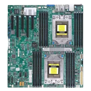
The primary mechanical and electrical advantage of multi-layer architectures lies in the integration of dedicated ground and power planes. These internal planes provide low-impedance return paths for high-speed signals, effectively shielding critical transmission lines from electromagnetic interference (EMI) and cross-talk. By strategically placing signal layers adjacent to continuous ground planes, design engineers can construct microstrip or stripline routing topologies that strictly adhere to target characteristic impedances (typically 50Ω single-ended and 85Ω to 100Ω differential pairs).
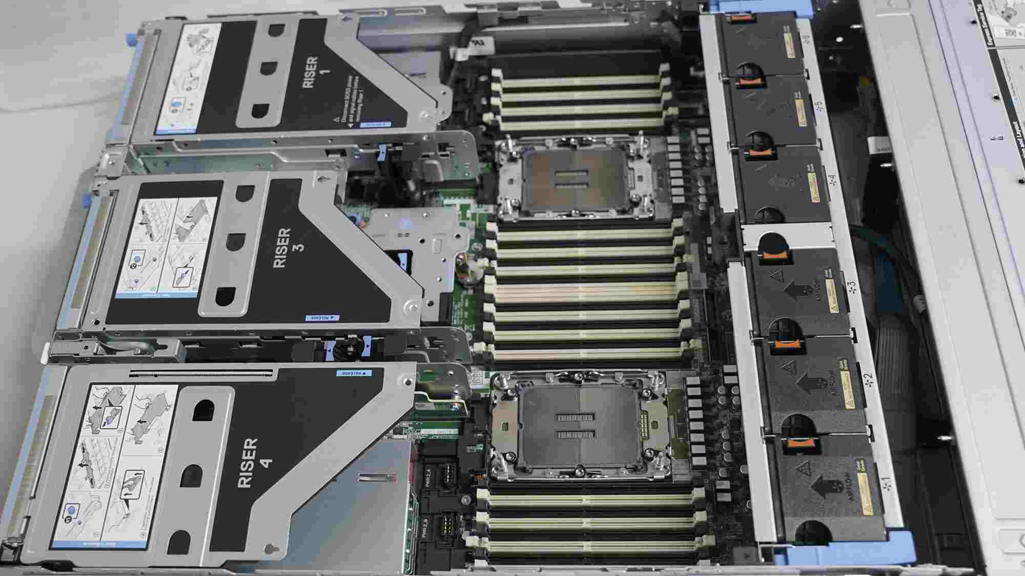
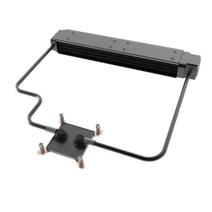
Furthermore, thermal management is heavily optimized in multi-layer structures. High-power components, such as multi-core processors, memory controllers, and power converters, dissipate significant amounts of heat. Internal solid copper planes act as lateral heat spreaders, transferring thermal energy away from local hot spots toward the edges of the board or dedicated cooling modules. Specialized vias, known as thermal vias, are placed beneath components to connect surface copper pads to internal thermal distribution planes, drastically lowering the overall junction temperature.
Strict control over track geometry, dielectric constants, and dielectric height is maintained to ensure reflection-less high-speed signal routing.
Engineered via arrays and thick inner copper layers distribute heat uniformly across the board to mitigate local thermal failure points.
Solid, uninterrupted copper planes prevent high-frequency radiation leakages and insulate internal circuits from external ambient noise.
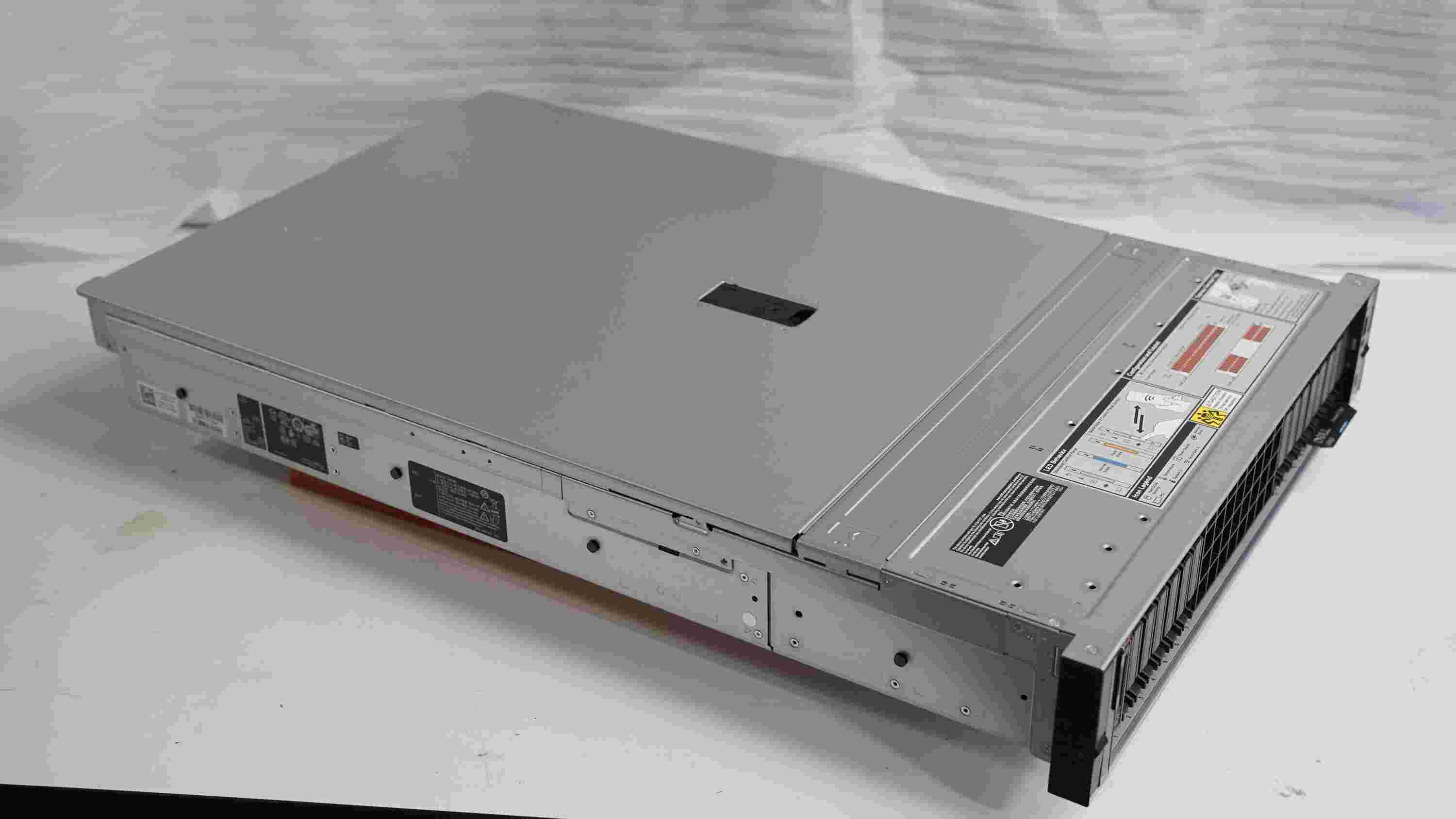
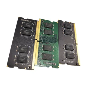
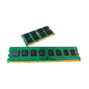
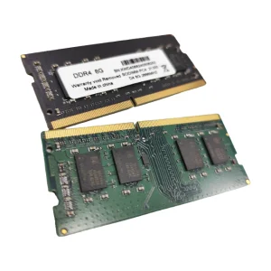
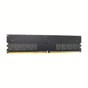
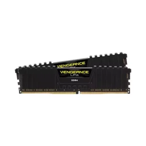
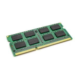
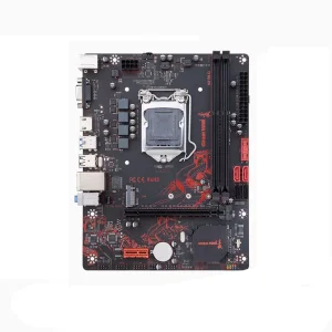
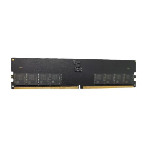
High-performance hardware configurations like servers, data centers, and advanced consumer desktops heavily rely on DDR5 and DDR4 memory modules. VoltDRAM Semiconductor has established itself as an industry leader in engineering high-reliability DRAM modules. The design of memory PCB substrates represents one of the most complex challenges in high-frequency multi-layer PCB manufacturing.
DDR5 modules operate at speeds starting from 4800MHz up to 6400MHz and beyond. At these transfer rates, signal rise times are incredibly sharp, meaning that even minor track length mismatches or impedance discontinuities will lead to bit errors, data corruption, or system instability. To control these phenomena, multi-layer PCBs for memory systems must utilize premium low-loss laminates (e.g., Megtron 6 or Nelco materials) and employ advanced manufacturing techniques:
VoltDRAM Semiconductor's R&D division has mastered these high-speed signal integrity techniques, combining them with robust thermal dissipation designs (such as copper-aluminum composite heatsinks) to deliver ultra-stable memory PCBs that excel in sustained high-throughput enterprise environments.
Years Industry Expertise
Annual Export Revenue
Dedicated R&D Engineers
New Products Annually
Global system integrators and technology enterprises choose Chinese multi-layer PCB manufacturers due to the unparalleled advantages of localized industrial ecosystems, engineering capacity, and logistical infrastructure. Southern China, especially the Pearl River Delta, houses the world's most concentrated electronics supply chain.
1. Material Access and Integrated Supply Chains: Within a 50-kilometer radius, factories have direct access to raw material manufacturers supplying copper clad laminates (CCL), copper foil, glass fabric, chemicals, epoxy resins, and electronic components. This proximity ensures that custom stack-up designs using specific high-Tg (glass transition temperature) or low-loss materials can be sourced and processed with minimal lead times.
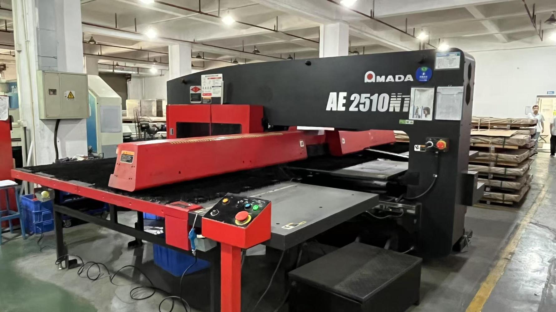
2. Advanced Machinery and Automation: Modern Chinese factories have heavily invested in high-precision automated manufacturing equipment. This includes LDI (Laser Direct Imaging) systems for fine line resolution down to 2 mil/2 mil (50um/50um), automated optical inspection (AOI) systems for defect checking, horizontal plating lines for uniform copper distribution in high-aspect-ratio holes, and multi-spindle CNC drilling machines.
3. Skilled Engineering Pools and OEM/ODM Adaptability: The abundance of experienced semiconductor and electronics manufacturing engineers allows factories to quickly review Gerber files for Design for Manufacturing (DFM) issues. Design adjustments, panelization schemes, and material recommendations are generated within hours, speeding up prototype iterations to full-scale mass production.
At VoltDRAM Semiconductor's manufacturing facilities, this localized efficiency translates to robust production capacities, letting the company handle diverse requirements from prototype multi-layer PCBs to high-density DDR5 memory modules for global export markets.
VoltDRAM Semiconductor offers end-to-end OEM and ODM services, serving clients in North America, Europe, Southeast Asia, and the Middle East. With facilities spanning 320–480㎡ and ISO-based quality management frameworks, we scale production smoothly from low-volume prototypes to mass runs.
We support a wide array of customized options, including:
By maintaining close partnerships with 600–1,500 supply chain partners, we ensure high quality, reliable supply chains, and fast delivery timelines.
Quality and reliability form the cornerstone of VoltDRAM Semiconductor's philosophy. High-speed multilayer PCBs and DDR5 server memory modules are placed under heavy physical and electrical strain during operation. Even a microscopic micro-crack or void in a copper via can trigger critical system failures.
To prevent field failures, our factory implements a comprehensive multi-stage testing protocol overseen by 35–80 dedicated quality inspectors:
The global electronics industry is moving toward higher integration and power density. Multi-layer PCB manufacturing must keep pace with these market developments:
VoltDRAM Semiconductor constantly tracks these industry trends, investing in advanced materials, process technologies, and training for our engineering teams to ensure we deliver high-performance, forward-looking solutions.
For standard prototype multi-layer PCBs (4 to 8 layers), the production lead time is typically 3 to 5 business days. For complex configurations (HDI, high layer count up to 32 layers, or specialty materials like Megtron), prototyping can take 7 to 10 days. Mass production orders generally ship within 15 to 25 business days, depending on material availability, layer counts, and surface finish options.
VoltDRAM manages signal integrity through meticulous PCB layout design, strict controlled impedance modeling, simulation tests, and high-performance base materials. We utilize tight-tolerance differential pairs, eliminate via stubs via backdrilling, and perform Automated Optical Inspection (AOI) alongside automated performance testing to ensure zero transmission loss and maximum signal stability.
For high-density designs with fine-pitch components (BGAs, micro-QFNs), we recommend ENIG (Electroless Nickel Immersion Gold) or ENEPIG (Electroless Nickel Electroless Palladium Immersion Gold). These finishes provide a flat coplanar surface, long shelf life, and outstanding solderability, protecting critical traces from oxidation.
Yes. VoltDRAM Semiconductor offers full turn-key OEM/ODM solutions, from layout engineering, component sourcing (ICs, capacitors, connectors), multilayer board fabrication, to surface mount assembly (SMT) and final functional verification.
We work closely with certified laminate suppliers, conducting incoming quality inspections (IQC) on parameters such as glass transition temperature (Tg), thermal expansion coefficient (CTE), and dielectric constant (Dk/Df). All raw material batches must match RoHS and REACH standards.
Standard board thickness is 1.6mm (0.063 inches), but we fabricate boards ranging from ultra-thin 0.4mm designs up to thick 3.2mm or 6.0mm backplanes for heavy industrial or complex rackmount server installations.
Rapid temperature swings generate physical stresses due to differing thermal expansion rates between copper, FR4, and epoxy resins. To prevent delamination, trace failure, and via fractures, we specify high-Tg resins (e.g., Tg170 or Tg180) and run boards through rigorous thermal cycle tests to verify product reliability.
To start your request, submit your Gerber files (RS-274X or OBD++ format) along with your stack-up specifications, Bill of Materials (BOM), and testing preferences. Our engineering team will return a detailed DFM review and pricing quotation within 24 hours.