Direct factory solutions optimized for Nagoya's tier-1 automotive radar subsystems, robotics automation controllers, and data storage arrays.
As the economic epicenter of Aichi Prefecture, the Chubu region surrounding Nagoya represents Japan's undisputed stronghold of heavy industrial manufacturing, advanced robotics, and automotive technology. Often dubbed the industrial heart of Japan, Nagoya hosts critical supply chain hubs for globally dominant automotive OEMs and tier-one aerospace suppliers. However, the region is currently undergoing a massive structural pivot toward Connected, Autonomous, Shared, and Electrified (CASE) mobility and cyber-physical automation. This paradigm shift requires hardware components to handle frequencies scaling from sub-GHz bands to millimeter-wave (mmWave) ranges exceeding 77 GHz.
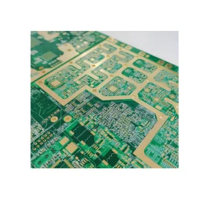
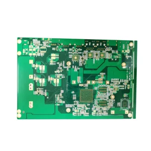
Within this highly demanding commercial ecosystem, high-frequency printed circuit boards (PCBs) act as the foundational substrate for next-generation systems. Whether it is advanced driver assistance systems (ADAS), V2X (vehicle-to-everything) communication modules, high-resolution automotive LiDAR, or automated guided vehicles (AGVs) operating inside Nagoya's advanced logistics hubs, the physical layers of these devices must guarantee zero-loss transmission profiles under harsh industrial conditions. Standard FR4 PCBs cannot support the data rate demands or the stringent signal integrity criteria of these newer applications, creating a massive demand for hybrid materials, microwave PTFE layers, and high-frequency stackups.
To succeed in the highly demanding Japanese market, high-frequency PCBs and computational modules must be engineered around localized application-specific conditions. In Nagoya, three major domains represent the bulk of critical electronic integration:
Integrated RF transceivers require ultra-thin, low-dissipation substrates (such as Rogers RO4350B or Shengyi S74397) to transmit and receive signals without phase distortions, maintaining precision in inclement winter weather across the Aichi prefecture.
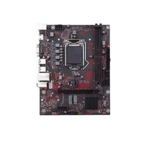
Multi-axis industrial robots deployed in automotive stamping and assembly plants rely on high-speed fieldbus interfaces and microprocessors requiring impedance-controlled multi-layer PCBs and thermal interface structures to withstand vibration and heat.
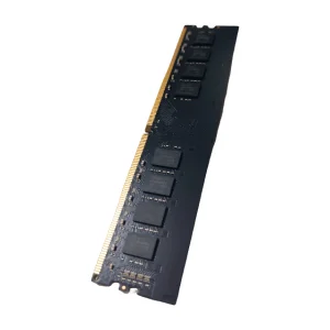
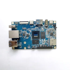
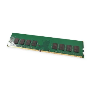
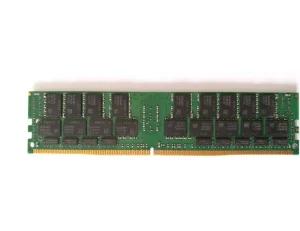
Real-time AI inference at the factory edge requires high-frequency DDR5 memory configurations, high-density processors (such as RK3588S IoT cores), and high-power dissipation systems with 200W-300W thermal capacities to avoid thermal throttling.
When processing signals in the 10 GHz to 80 GHz range, standard glass-epoxy (FR4) substrates exhibit high dielectric loss (dissipation factor, Df) and inconsistent dielectric constant (Dk) stability across varying temperatures. Utilizing a Rogers-Shengyi hybrid stack-up reduces board costs while maintaining ultra-low loss on the critical RF tracing layers. This allows engineers to place RF front-end components and high-speed memory arrays on a single, cost-effective printed circuit assembly.
Navigating the electrical boundaries: from low-loss hybrid stack-ups to high-speed DDR5 memory topologies.
In high-speed communication systems and edge server computing, signal losses can easily compromise systemic throughput. To address these problems, the technical roadmap of modern factories revolves around several critical physical layer optimizations:
At high frequencies, the "skin effect" forces electrical current to travel primarily on the surface of the copper traces. Rough copper profiles create longer path lengths, which directly increases conductor losses. Modern manufacturers use rolled copper or very low-profile (VLP) electrodeposited copper foils to minimize this effect. Additionally, using advanced thermoset hydrocarbon and ceramic laminates (such as Rogers RO4350B, RO4003C, or Taconic RF-35) ensures consistent performance across temperatures. Dielectric constants are kept within tolerances of ±0.05, and dissipation factors are limited to under 0.003 at millimeter-wave ranges.
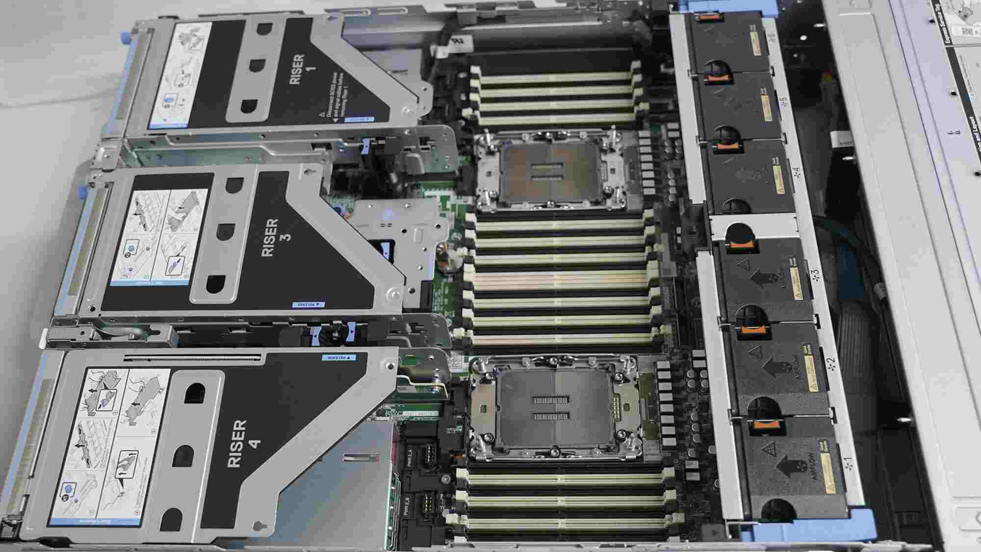
Routing density on modern motherboard systems (like the RK3588S development boards or high-density server computing boards) requires complex vertical connections. Utilizing Laser Direct Structuring (LDS) and stacked microvias (via-in-pad structures) minimizes capacitive loading and impedance discontinuities. This allows engineers to achieve trace widths and spacings under 3 mil (75 µm), which is essential for routing 32-bit and 64-bit wide parallel high-speed buses without crosstalk or signal integrity distortion.
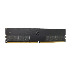
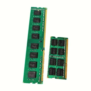
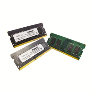
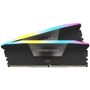
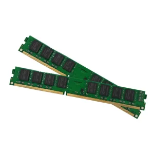
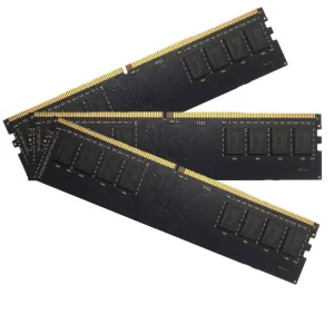
Transitioning from DDR4 to DDR5 introduces unique challenges, including on-board Power Management ICs (PMICs) on the memory module itself and dual 32-bit subchannels. Because signal speeds reach 5600MT/s and higher, maintaining quiet, stable power rails is critical. VoltDRAM Semiconductor's R&D engineering optimizes PDN (Power Delivery Network) impedance profiles to prevent transient noise from coupling into high-speed data buses. Through rigorous electromagnetic simulator models, we design robust ground return paths and decoupling capacitor placements to limit jitter and preserve clean data eyes.
How our integrated factory ecosystem delivers rapid prototyping and high-volume scalability directly to Nagoya.
Global electronic manufacturing demands speed and reliable quality, two priorities that can conflict. With our facility based in Shenzhen's technology cluster, we have optimized the logistics and engineering path to Nagoya. The Port of Nagoya and Chubu Centrair International Airport act as direct entry points, allowing for seamless shipping times. This logistics path supports Japanese manufacturers running lean inventory systems (Just-in-Time).
By using local component suppliers, our factory accelerates prototyping. High-frequency RF designs require multiple iterations to tune microstrip lines and coplanar waveguides. While domestic Japanese prototyping can take weeks and require high costs, our facilities deliver prototype PCBs in 3-5 working days. This rapid turnaround is paired with detailed cross-section analyses and TDR impedance reports to confirm design requirements before volume production.
Once prototypes are approved, our automated optical inspection (AOI) systems and in-circuit testing (ICT) ensure the transition to mass production is seamless. Because we process raw substrates, multi-layer lamination, and SMT assembly under one roof, we minimize transfer delays. This integrated approach allows Nagoya-based system integrators to scale up production without managing multiple vendors or dealing with shipping delays.
Our strict focus on trace control and testing guarantees high yield rates, even for complex multi-layer boards. This balance of speed, performance, and cost-efficiency is why engineering teams across Nagoya choose our manufacturing services for their industrial computing needs.
VoltDRAM Semiconductor Co., Ltd. is a professional DDR5 memory manufacturer specializing in high-performance DRAM solutions for servers, PCs, and data center applications. The company was registered between 2015–2018 and has rapidly developed into a reliable global supplier in the memory industry.
Our manufacturing facility covers an area of approximately 320–480㎡, equipped with advanced production and testing lines. We generate an annual export revenue of around USD 8–18 million, with 6–9 years of export experience and 8–15 years of industry expertise in semiconductor memory development and manufacturing.
Quality is at the core of VoltDRAM. We implement strict ISO-based quality management systems, combined with automated optical inspection (AOI), electrical performance testing, burn-in testing, and reliability stress testing to ensure stable product performance. Our quality control team consists of 35–80 experienced inspectors, ensuring every batch meets international standards.
With a strong international trade background, VoltDRAM mainly serves markets in North America, Europe, Southeast Asia, and the Middle East. We maintain long-term cooperation with over 600–1,500 supply chain partners, supporting a stable and efficient production ecosystem.
Our customers include OEM/ODM brands, system integrators, data center operators, and industrial computer manufacturers. We have strong R&D capabilities focused on high-speed DDR5 architecture optimization, signal integrity improvement, and power efficiency design. We also provide full customization options, including PCB design, memory capacity configuration, frequency tuning, and branding solutions.
Each year, we launch approximately 120–450 new product variants, supported by a dedicated R&D team of 60–300 engineers. Our innovation-driven approach allows us to continuously deliver competitive and high-performance memory solutions to global customers.
Ensuring hardware reliability through rigorous validation and international certification frameworks.
Navigating the compliance requirements of the Japanese electronics market demands close attention to regulatory standards. In Japan, electrical products must meet specific certification pathways. Our high-frequency PCBs and computing systems are manufactured under strict processes to comply with global guidelines. From materials sourcing to final packaging, we ensure our products align with standard green initiatives and RoHS restrictions.
For systems that interface directly with the main electrical grid, we provide assistance to ensure your complete assembly meets necessary PSE (Product Safety Electrical Appliance & Material) and VCCI (Voluntary Control Council for Interference) noise emissions standards. This is particularly critical for industrial welding inverters and heavy-duty factory power management systems that generate significant electromagnetic noise.
Answers to common engineering questions regarding layout optimization and thermal management.
Pure PTFE-based Rogers substrates offer excellent dielectric stability, but they are expensive and can be mechanically soft during assembly. By laminating high-frequency Rogers prepregs onto a stable, high-TG Shengyi FR4 core, we balance performance and cost. This hybrid approach keeps critical high-speed traces on the top layer, while ground lines and power planes are routed through the FR4 layer. This design reduces board costs by up to 45% without compromising signal integrity.
DDR5 runs at high speeds, which can generate electromagnetic noise. We mitigate this by using micro-stripline designs sandwiched between reference ground planes. This layout shields the signal paths and keeps routing short. We also use 3D electromagnetic simulators to check impedance mismatches before production, ensuring cleaner signal lines and reliable data processing at high clock rates.
We subject all automotive-grade assemblies to Interconnect Stress Testing (IST) to check for thermal fatigue in copper vias. We also perform Highly Accelerated Life Testing (HALT) and High-Temperature Storage Life (HTSL) tests. These steps ensure that solder joints and copper layers do not crack under vibration or temperature swings, keeping automotive systems reliable.
Yes. We support custom designs and firmware updates, including custom SPD configurations for memory modules. This includes setting custom latency profiles, memory speeds, and serial numbers. We also offer options for physical marking, custom PCB colors, and custom cooling shrouds to fit your company's branding.
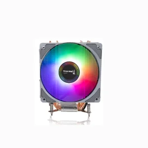
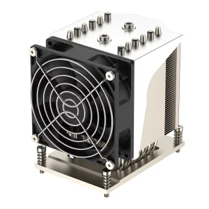
Our cooling modules use high-density aluminum fins and direct-contact copper heat pipes to manage high thermal levels. They are rated for heat densities up to 85 Watts per square centimeter. This allows them to handle demanding CPU loads on server architectures without thermal throttling, maintaining stable performance in 2U and 4U chassis systems.
Every shipment includes a detailed inspection packet containing cross-section microsections, solderability test reports, copper thickness measurements, and impedance test results. We also provide compliance certificates for RoHS and REACH, along with material data sheets to verify electrical parameters.
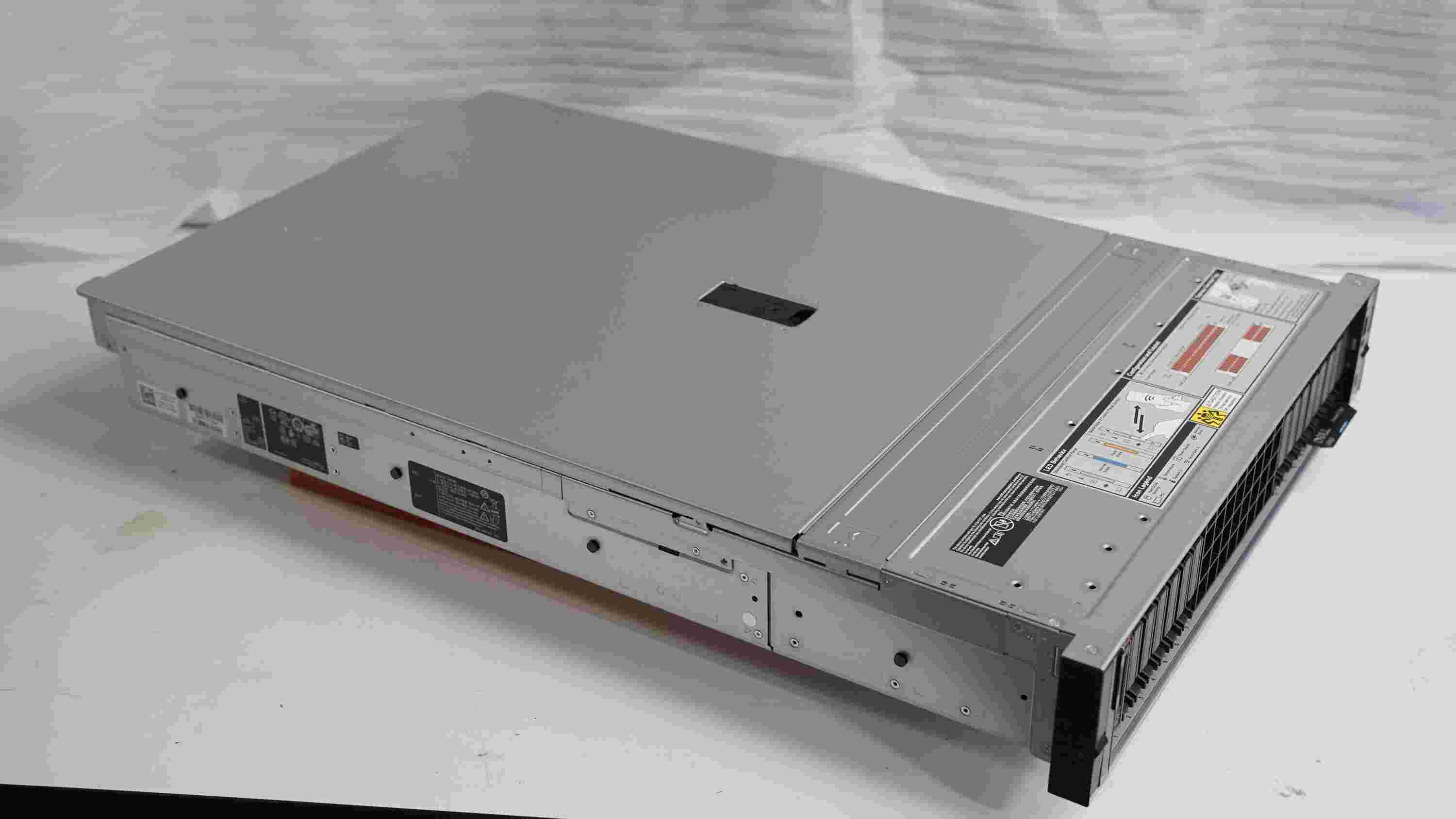
High-reliability DRAM modules and cooling systems designed to optimize industrial servers and workstation fleets.
Our ISO-certified manufacturing space incorporates automated optical inspection, electrical validation platforms, and chip testing setups to ensure consistent product delivery.