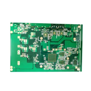
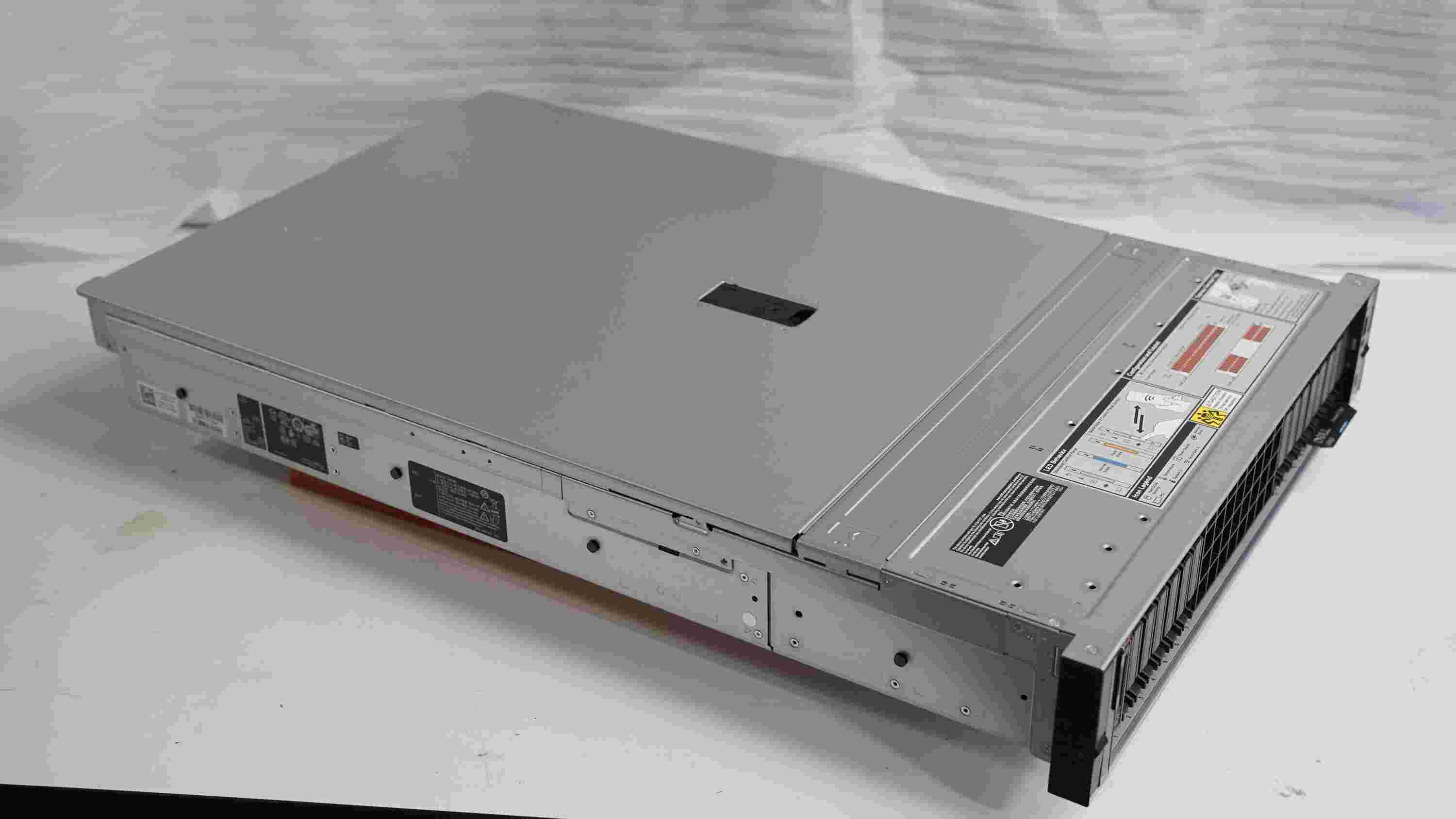
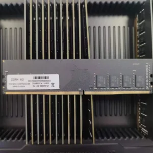
High-reliability hardware designed to integrate seamlessly with German industrial automation, manufacturing lines, and stencil alignment configurations in Hamburg.
As Northern Europe's leading logistics and industrial hub, Hamburg houses major electronics development, aerospace manufacturing, and maritime technologies. High-precision Surface Mount Technology (SMT) assembly is at the heart of these sectors, driving an ongoing requirement for advanced laser-cut stencils. Hamburg’s industrial clusters, including the aviation center in Finkenwerder and research parks in Harburg, depend on rapid-turnaround, micro-aperture printing solutions to populate PCBs for flight-control systems, high-speed marine radar, and automated cargo-handling machines.
A key challenge for electronic contract manufacturers (EMS) in Hamburg is maintaining assembly yields when working with complex modern components. Components such as 01005 passives, ultra-fine-pitch Ball Grid Arrays (uBGAs), and dual-row QFNs require highly controlled solder paste volume deposition. Standard mechanical or basic laser-etched stencils no longer deliver the necessary tolerances. Modern exporters serving Hamburg must supply laser stencils manufactured with precision laser platforms, specialized raw materials like high-tension fine-grain stainless steel, and cutting-edge surface finishes.
High-quality laser stencils rely on precise execution across design, material selection, and laser calibration. Stencil production starts with Gerber file preparation, where engineers adjust apertures using dynamic scaling factors to account for solder paste release characteristics. Using advanced CAM software, apertures are customized with micro-adjustments such as "home-plate" or "C-cut" geometries to minimize solder balling and bridging on critical pins.
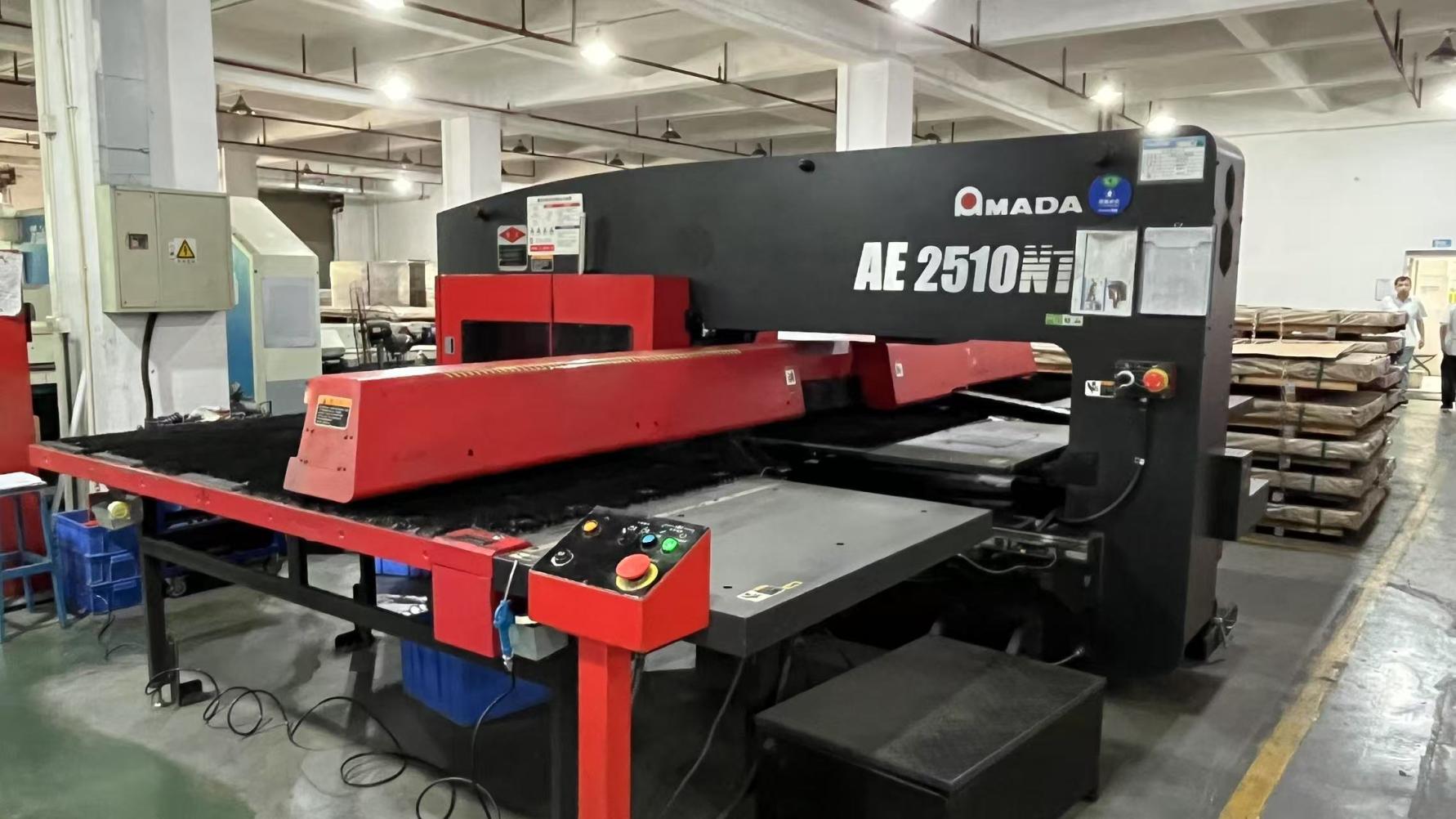
Once the design is optimized, the stencils are cut using specialized fiber laser systems. Fiber lasers feature a highly concentrated spot size (typically under 20 microns) and clean edge-cutting capabilities, producing smooth vertical aperture walls. This is critical for maintaining paste release efficiency. In contrast to traditional CO2 lasers, fiber laser systems minimize the heat-affected zone (HAZ), reducing the risk of thermal distortion and ensuring accurate aperture arrays across large printing areas.
| Stencil Type | Cutting Accuracy | Best Applied For | Paste Release Efficiency |
|---|---|---|---|
| Standard Laser Cut Stencil | ±3 µm | Standard SMT components (0402, QFP, SOIC) | Moderate (70-80%) |
| Electro-Polished Laser Stencil | ±2 µm | Fine-pitch components (0201, BGA down to 0.4mm pitch) | High (80-90%) |
| Nano-Coated Laser Stencil | ±2 µm | Ultra-fine-pitch (01005, WLCSP, 0.3mm pitch BGA) | Excellent (95%+) |
| Step Stencils (Up/Down) | ±4 µm | Mixed density layouts requiring varied paste volume | Variable based on pocket depth |
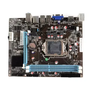
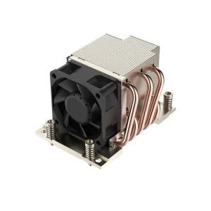
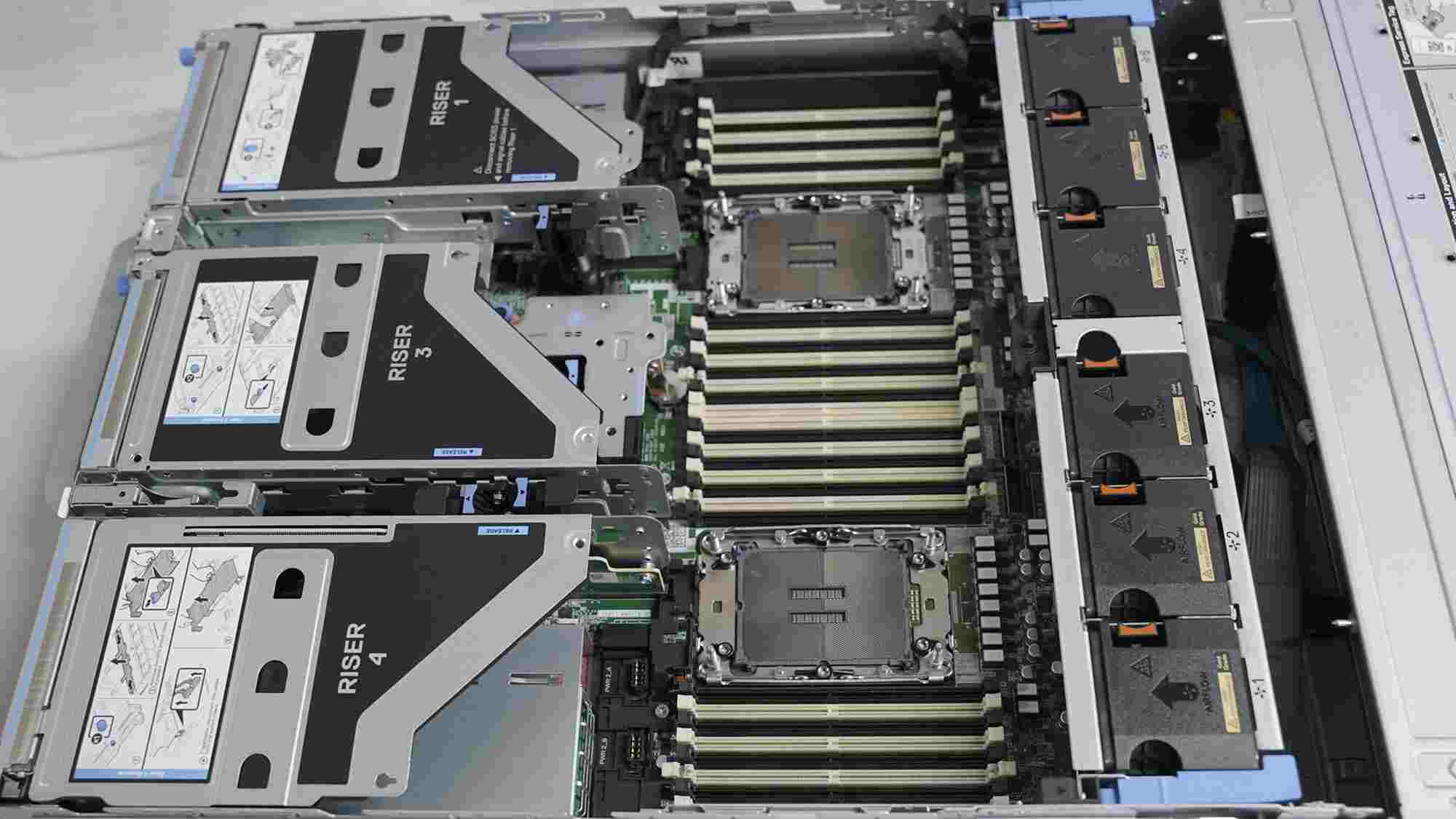
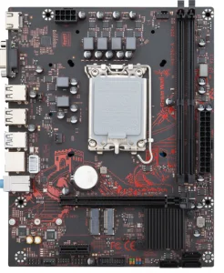
High-end PCB fabrication hardware and thermal management systems to support demanding assembly projects in Germany.
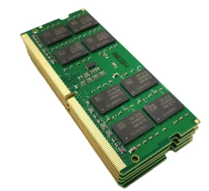
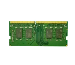
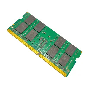
Pioneering advanced memory architecture, precision semiconductor design, and global component supply systems.
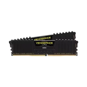
VoltDRAM Semiconductor Co., Ltd. is a professional DDR5 memory manufacturer specializing in high-performance DRAM solutions for servers, PCs, and data center applications. The company was registered between 2015–2018 and has rapidly developed into a reliable global supplier in the memory industry.
Our manufacturing facility covers an area of approximately 320–480㎡, equipped with advanced production and testing lines. We generate an annual export revenue of around USD 8–18 million, with 6–9 years of export experience and 8–15 years of industry expertise in semiconductor memory development and manufacturing.
Quality is at the core of VoltDRAM. We implement strict ISO-based quality management systems, combined with automated optical inspection (AOI), electrical performance testing, burn-in testing, and reliability stress testing to ensure stable product performance. Our quality control team consists of 35–80 experienced inspectors, ensuring every batch meets international standards.
With a strong international trade background, VoltDRAM mainly serves markets in North America, Europe, Southeast Asia, and the Middle East. We maintain long-term cooperation with over 600–1,500 supply chain partners, supporting a stable and efficient production ecosystem.
Our customers include OEM/ODM brands, system integrators, data center operators, and industrial computer manufacturers. We have strong R&D capabilities focused on high-speed DDR5 architecture optimization, signal integrity improvement, and power efficiency design. We also provide full customization options, including PCB design, memory capacity configuration, frequency tuning, and branding solutions.
Each year, we launch approximately 120–450 new product variants, supported by a dedicated R&D team of 60–300 engineers. Our innovation-driven approach allows us to continuously deliver competitive and high-performance memory solutions to global customers.
VoltDRAM is committed to becoming a trusted global partner in the DDR5 memory industry, delivering stable, fast, and efficient memory products for the next generation of computing systems.


For system integrators, OEM brands, and data center operators in Hamburg, procuring SMT stencil tooling involves several key factors: precision, speed, compatibility, and cost-efficiency. Modern production lines run at high speeds, and stencil failure leads to downstream defects (e.g., solder bridging or insufficient wetting). Consequently, SMT engineers require stencils that minimize down-time for under-screen cleaning.
This is where high-performance materials and advanced finishes play a key role. Standard laser-cut stencils are often upgraded with Electro-Polishing (EP) or hydrophobic nano-coatings. Electro-polishing uses a chemical-electrical bath to smooth microscopic roughness along the laser cut path. Nano-coatings create a hydrophobic and flux-phobic barrier on the stencil's contact side. This limits solder paste transfer to the stencil's underside, reducing clean cycles from every 3-5 boards to every 25-50 boards, significantly increasing overall production capacity.
Solder paste printing performance is heavily influenced by stencil thickness. Exporters serving Hamburg offer standard stencil foils ranging from 80 microns to 150 microns. The selection depends on the paste volume requirements of the components. Modern dense board designs containing both large power-handling components and miniature signal processors require varying thicknesses on a single board, which is resolved using Step Stencils.
Step-up stencils feature thicker local zones to deliver more solder paste to connectors or power transistors. Step-down stencils use chemical milling or laser ablation to create thinner zones, reducing paste volume for fine-pitch BGAs. Every step stencil undergoes meticulous 3D optical inspection to verify depth consistency, ensuring print reliability.
| Technical Parameter | Specification Limit | Method of Control | German Industrial Benchmark |
|---|---|---|---|
| Aperture Positional Tolerance | < ±5 µm | Linear scale encoder monitoring | DIN EN 61191 Compliant |
| Foil Thickness Uniformity | ± 3% | Micrometer & Ultrasonic Gauging | IPC-7525B Standard |
| Wall Surface Roughness (Ra) | < 0.5 µm (after EP) | Laser Profilometer Scanning | High-Reliability Class 3 Electronics |
| Tension Stability | > 40 N/cm | Mechanical Tension Testing | Automotive SMT Line Ready |
Logistics reliability is a key factor when exporting stencils to Hamburg. SMT production schedules are highly time-sensitive. Standard laser-cut stencils are typically dispatched within 24 to 48 hours of design sign-off. Utilizing air freight directly to Hamburg Airport (HAM) or shipping through European logistics hubs ensures express components reach facilities within Northern Germany quickly.
Furthermore, products comply with all European environmental and industrial standards. Compliance with the RoHS Directive (2011/65/EU) and REACH Regulations (EC 1907/2006) is fully certified. The steel foils, frames, and adhesives used are non-hazardous, ensuring smooth customs clearance through the Port of Hamburg (Hafen Hamburg) and reliable integration into German manufacturing chains.
A comprehensive range of industrial computing boards, memory components, and thermal systems built for heavy-duty commercial deployment.
Find expert answers to key technical questions about stencil selection, materials, quality standards, and shipping options for Hamburg.
Stencil thickness selection is guided by the aspect ratio (width of aperture / thickness of foil) and the area ratio (area of aperture opening / area of aperture walls). According to IPC-7525 guidelines, the area ratio must be greater than 0.66 to ensure reliable paste release. For boards with mixed technologies, step-up or step-down stencils are used to vary the thickness locally across different regions.
Electro-polishing is an electrochemical process that smooths the internal walls of the laser-cut apertures. It removes micro-burrs and reduces wall roughness. This lowers the friction between the solder paste and the aperture walls during stencil release, decreasing paste residues and improving print consistency on fine-pitch components.
Fine-grain steel foils (grain size of 1 to 5 microns, compared to 15 to 25 microns in standard steel) offer higher mechanical strength and flatter surfaces. This grain structure allows for smoother laser cuts and prevents deformation during tensioning, ensuring consistent stencil flatness and aperture shape across high-volume production runs.
Hydrophobic and flux-phobic nano-coatings are typically applied during stencil fabrication. They form a thin, durable layer that repels flux binders. Under normal production conditions with soft cleaning wipes, a quality nano-coating lasts for roughly 30,000 to 50,000 printing cycles before requiring reapplication or replacement.
Customers provide design data in Gerber, ODB++, or DXF formats. Our engineering team reviews the files using specialized CAM systems, applying adjustments for solder paste volume, fiducial alignment, and panel layouts based on the target stencil frame configuration.
Every stencil undergoes Automated Optical Inspection (AOI) to check aperture geometry, dimensions, and positioning relative to the Gerber file. Visual inspections are also conducted to verify surface finish, frame tension, and overall dimensional accuracy before the stencil is packed for shipping.
Stencils are packaged in custom-fit wooden crates or shock-resistant double-wall cardboard boxes. The stencil frame is secured with foam inserts, and the foil surface is protected by plastic sheets to prevent scratches, puncture damage, or environmental exposure during international transit.
Fabrication takes 24 to 48 hours from design approval. Using express air freight services, transit to Hamburg takes between 3 to 5 business days, ensuring minimal delay for local manufacturing operations.
Partner with an experienced laser stencil and semiconductor hardware exporter. Contact our engineering team for a customized technical quote and Gerber design review.