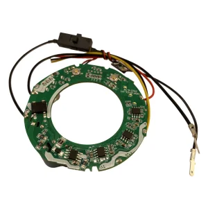
Engineered to integrate seamlessly with high-precision laser stencils on modern automated surface mount lines.
Seattle and the wider Pacific Northwest region—historically celebrated as the "Silicon Forest"—represent one of the world's most sophisticated clusters of high-reliability aerospace manufacturing, cloud server infrastructure, medical electronics, and pioneering consumer hardware. The engineering ecosystem spanning Seattle, Bellevue, Redmond, and Kent requires PCB assembly technologies of the highest fidelity. In these complex supply chains, the production of precision electronics begins with a single, foundational component: the SMT Laser Stencil.
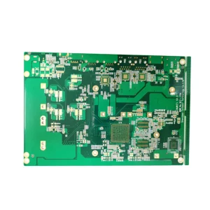
From commercial aviation avionics to the dense blade servers that power global cloud services, the demands placed on electronic component assemblies are exceptionally stringent. Seattle electronics manufacturing services (EMS) providers and original equipment manufacturers (OEMs) require laser stencils engineered to resolve the micro-fine-pitch component placements required by modern high-density interconnect (HDI) designs. Whether implementing 01005 passives, 0.3mm pitch BGAs, or heavy copper power-supply planes, the accuracy of the solder paste deposition process controls the end-to-end yield of the manufacturing line.
The global surface mount technology (SMT) landscape is undergoing rapid, structural evolution. As computational power requirements increase, electronics design engineers are pushed toward severe component miniaturization. This trend necessitates that stencils perform far beyond historical tolerances. Laser stencils have transitioned from standard stainless steel foils to high-precision laser-cut foils with advanced hydrophobic nano-coatings.
Global procurement teams in the Pacific Northwest evaluate partners using a multi-factor risk-reward framework. A reliable supplier must offer more than low pricing; they must serve as an engineering partner capable of reviewing Gerber data, identifying potential design-for-manufacturability (DFM) errors, and fabricating high-yield SMT stencils within accelerated timelines. Because SMT lines incur high downtime costs, stencil precision directly correlates with overall operational equipment effectiveness (OEE). High-quality laser stencils minimize rework, reduce the incidence of solder balling, and help secure high margins on high-reliability assemblies.
The modern Chinese manufacturing sector has evolved beyond simple high-volume output to become a hub for automated Industry 4.0 manufacturing. The manufacturing infrastructure utilizes advanced fiber laser cutting machines, multi-axis motion control stages, and automated optical inspection (AOI) systems integrated directly into the production line. This level of digitalization allows for rapid data transfer from Gerber design files directly to the laser cutting path, minimizing human intervention and ensuring consistent dimensional accuracy across multiple stencil batches.
Additionally, supply chain clustering in centers like Shenzhen and Dongguan facilitates rapid sourcing of high-grade raw materials, including fine-grain stainless steel foils and advanced frame mounts. Working with an experienced exporter enables Seattle-based engineering teams to access advanced manufacturing capacities with short lead times. Combined with reliable international air express networks, a custom-engineered stencil can be processed and delivered from the factory floor to a Seattle assembly facility in 3 to 5 business days.
Precision-cut laser stencils find application across several distinct technology sectors within the Seattle metropolitan area:
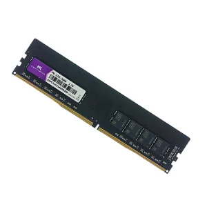
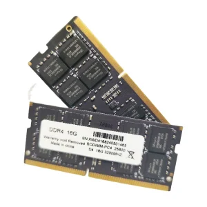
VoltDRAM Semiconductor Co., Ltd. is an established manufacturer specializing in high-performance DRAM memory solutions and advanced SMT design integration. Serving global data centers, servers, and PC hardware sectors, our operations span the semiconductor and PCBA fabrication pipelines. Founded between 2015–2018, VoltDRAM has grown to become a reliable partner in the electronic component supply chain.
Operating a manufacturing facility of approximately 320–480㎡, the plant is outfitted with modern production and testing configurations. We generate an annual export revenue of USD 8–18 million, backed by 6–9 years of export experience and 8–15 years of industry expertise in semiconductor memory development and high-density PCB/SMT board assembly techniques.
Quality assurance is maintained through ISO-based quality management systems, combined with automated optical inspection (AOI), electrical performance testing, burn-in testing, and reliability stress testing to verify stable hardware operation. The quality control group consists of 35–80 experienced inspectors, ensuring every batch meets international standards.
VoltDRAM serves key markets in North America, Europe, Southeast Asia, and the Middle East, maintaining long-term cooperation with 600–1,500 supply chain partners. This network enables us to secure reliable raw materials and coordinate rapid logistics directly to key tech hubs like Seattle. Our clients include OEM/ODM brands, system integrators, data center operators, and industrial computer manufacturers.
Supported by a dedicated R&D team of 60–300 engineers, we launch approximately 120–450 new product variants annually. This continuous development cycle ensures our memory solutions and SMT board integration technologies align with evolving industry standards.
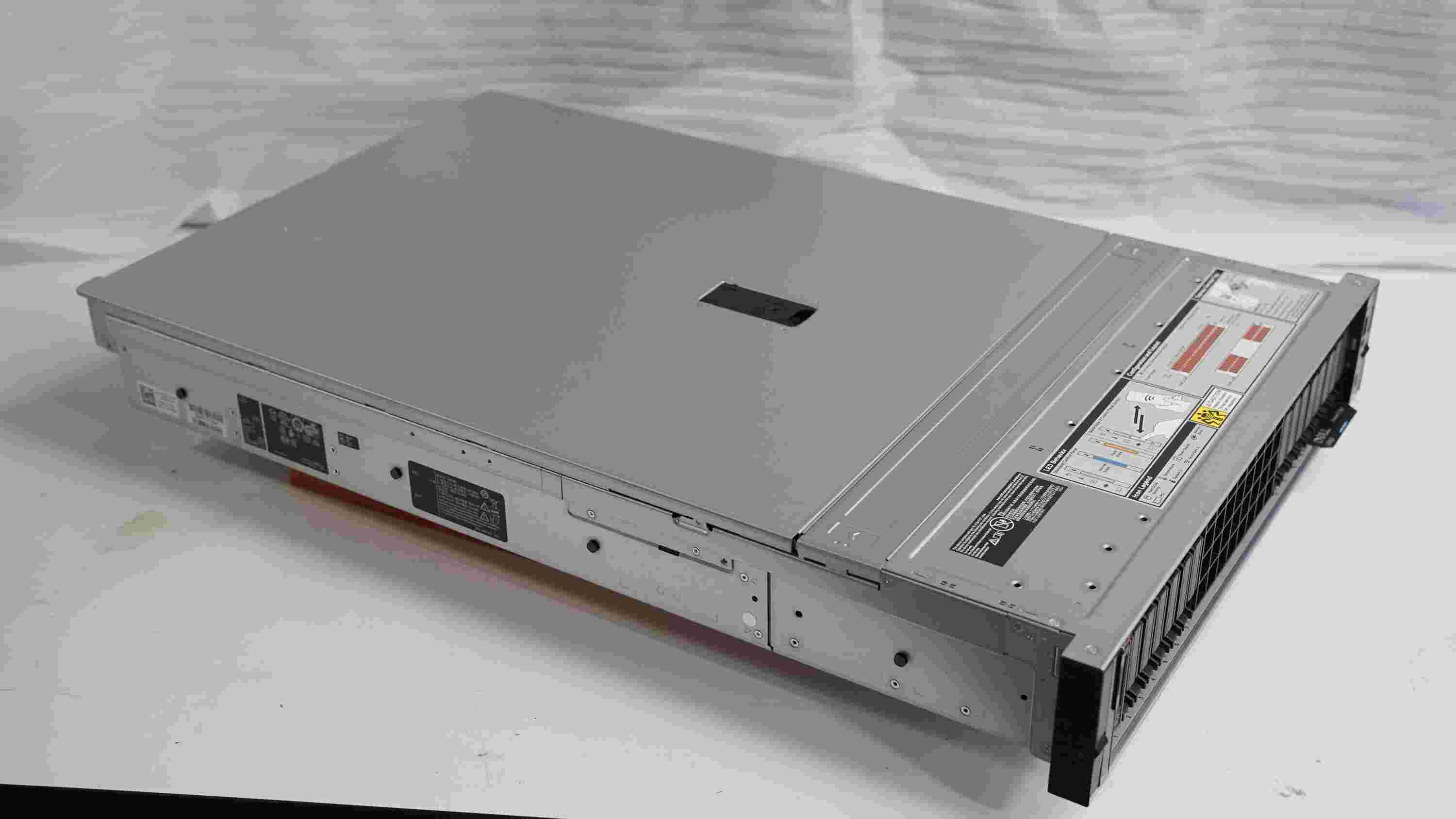
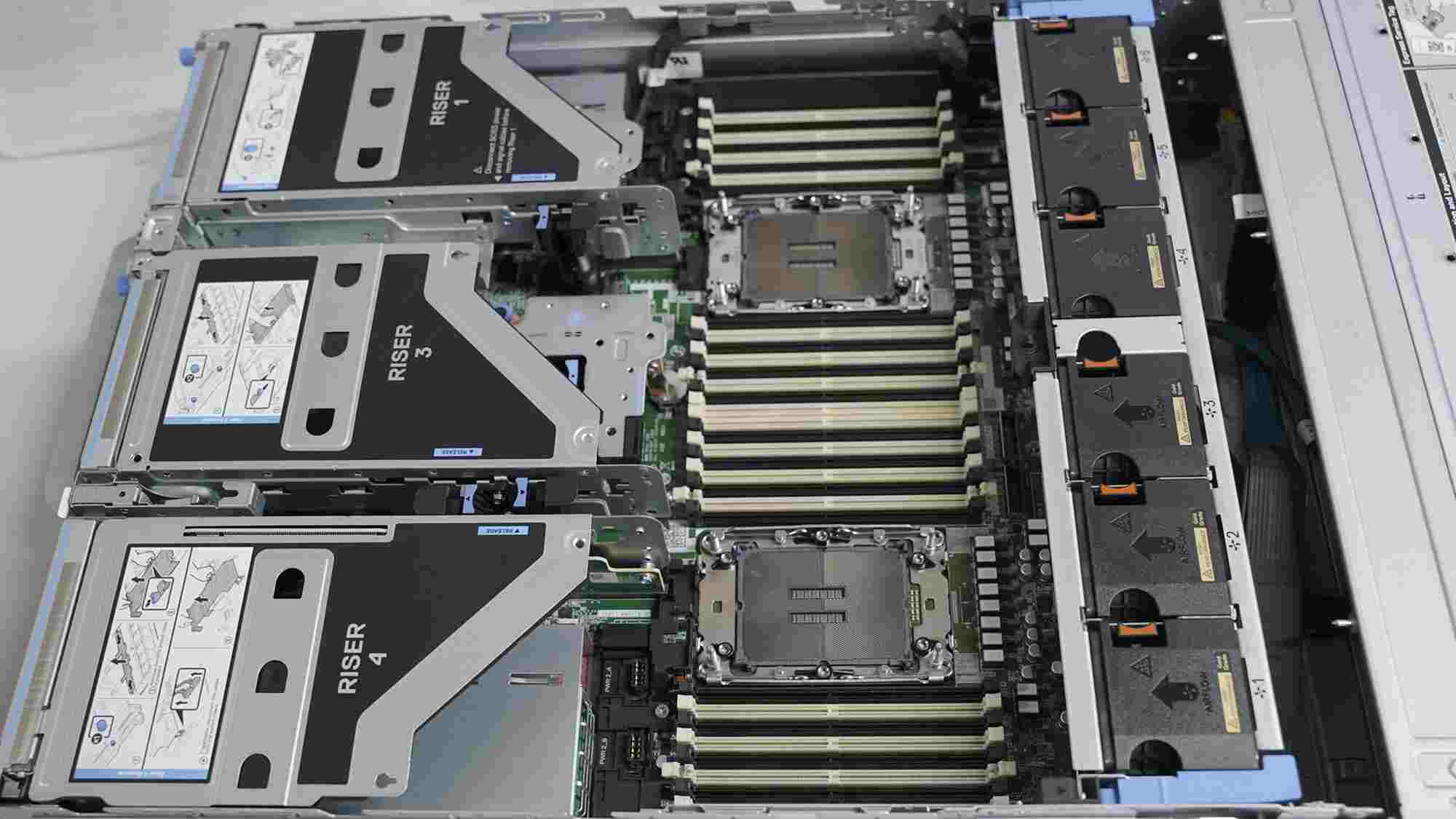


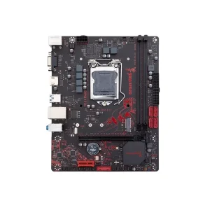
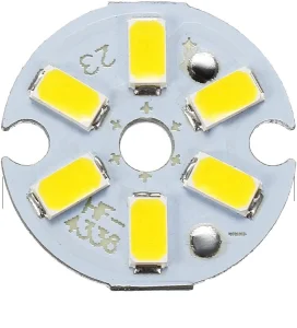
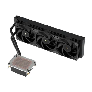
High-reliability server and system components designed for enterprise integration, featuring SMT precision layouts.
Addressing common engineering challenges and procurement requirements for Seattle-based electronic hardware programs.
Laser-cut stencils are manufactured from high-grade stainless steel foils using a CNC-controlled fiber laser, achieving high aperture positional accuracy. They are cost-effective, support short lead times, and are suitable for the majority of standard SMT designs down to 0.4mm pitches. Electroformed stencils are created atom-by-atom via nickel electrodeposition, producing smooth aperture walls and a natural gasket effect. While electroformed stencils offer superior paste release for ultra-fine-pitch designs (sub-0.3mm BGA), modern laser-cut stencils combined with nano-coatings provide comparable release performance at lower costs and with faster turnaround times.
The Area Ratio (AR) is calculated as the area of the aperture opening divided by the surface area of the aperture walls. For rectangular apertures, AR = (L × W) / [2 × T × (L + W)], where T is the stencil thickness. According to standard IPC-7525 guidelines, to ensure a complete release of solder paste (more than 70% transfer efficiency), the Area Ratio must remain above 0.66. If the ratio falls below this threshold, paste sticking occurs, resulting in insufficient solder joints. Stencil thicknesses must be adjusted or step-stencils designed when mixing fine-pitch components with larger, high-volume power components.
Step stencils are used when a single PCB design contains components with divergent solder paste volume requirements. A step-up stencil localizes thicker areas (e.g., transitioning from 0.12mm to 0.15mm) to supply additional paste volume to large connectors or power devices. A step-down stencil thins localized sections (e.g., from 0.12mm down to 0.08mm) to prevent solder bridging on fine-pitch components like QFNs, micro-BGAs, or 01005 passives. This approach allows manufacturers to optimize solder paste volume without compromising layout density.
Nano-coatings apply an ultra-thin (typically 2-4nm), hydrophobic and oleophobic layer to the stencil's contact side and inside the aperture walls. This coating reduces the friction coefficient between the solder paste and the metal, improving paste transfer efficiency. It prevents paste from bleeding under the stencil onto adjacent pads, which reduces bridging defects. For SMT production runs, nano-coatings reduce the required under-stencil wipe frequency from every 3-5 prints to every 15-20 prints, increasing line throughput and reducing consumable usage.
Quality control begins with CAD data verification using DFM checks to identify potential IPC violations before cutting. Post-laser cutting, stencils undergo Automated Optical Inspection (AOI) to verify aperture dimensions and edge quality. VoltDRAM packages stencils in heavy-duty, reinforced crates to prevent warping during transport. Leveraging close proximity to regional logistics hubs and partners, we coordinate express air shipment directly to Seattle-Tacoma International Airport (SEA). This pipeline enables Seattle customers to receive production-ready stencils in 3 to 5 business days from order placement.
We accept standard Gerber file formats, including Gerber RS-274X and Gerber X2, alongside ODB++ databases. The files should include the solder paste layers (typically .GTP for top paste, .GBP for bottom paste), silkscreen layers, and board outline layers to verify placement orientation. If step-stencils or custom aperture adjustments are required, design files should include a detailed drawing indicating the step areas, depths, and modifications needed.
Integrate advanced laser-cut stencil accuracy with high-reliability semiconductor components. Contact our engineering team for DFM verification, technical quotes, or customized SMT stencil tooling options.