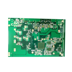
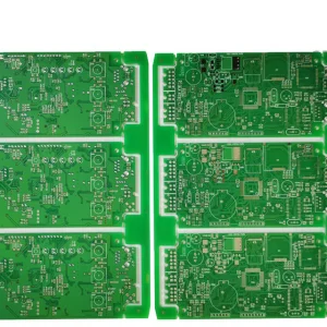
As the epicenter of global technology innovation, San Francisco and the broader Bay Area demand more than just standard circuit board manufacturing. The shift towards AI-driven hardware, 5G telecommunications, and high-performance computing (HPC) has catalyzed a need for advanced Multi-layer Circuit Board fabrication that pushes the boundaries of signal integrity, thermal management, and miniaturization.
VoltDRAM Semiconductor Co., Ltd. bridges the gap between Asian manufacturing efficiency and San Francisco’s rigorous engineering standards. Our multi-layer solutions—ranging from 4 to 32+ layers—are specifically engineered for the high-frequency requirements of the modern tech landscape. By leveraging Information Gain from years of R&D, we offer localized support that understands the specific compliance needs of Northern California’s aerospace, medical, and data center industries.
Utilizing micro-vias and laser drilling technology to maximize wiring density, essential for San Francisco's wearable tech and mobile device startups.
Advanced metal core and heavy copper multi-layer boards designed to dissipate heat in AI GPU clusters and high-power industrial inverters.
Custom impedance control and low-loss materials (like Rogers and Isola) to ensure ultra-fast data transmission for 6G and satellite communications.
"Our localized presence in San Francisco ensures that design engineers can transition from prototype to mass production without the typical pitfalls of cross-border logistics."
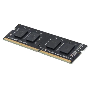
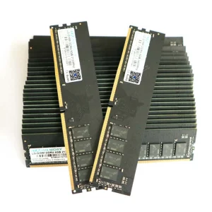
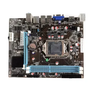
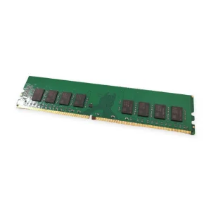
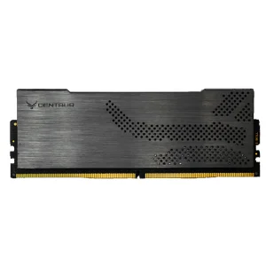
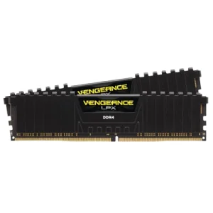
VoltDRAM Semiconductor Co., Ltd. is a professional DDR5 memory and PCB manufacturer specializing in high-performance DRAM solutions for servers, PCs, and data center applications. Registered between 2015–2018, we have rapidly developed into a reliable global supplier.
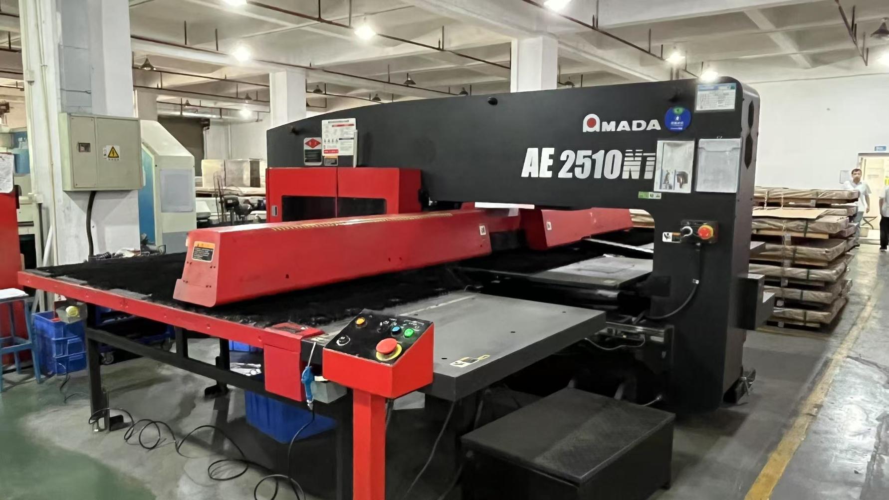
Our manufacturing facility covers 320–480㎡, equipped with advanced AOI and reliability stress testing. With an annual export revenue of USD 8–18 million, we support the North American market with precision-engineered Multi-layer Circuit Boards that meet international standards.
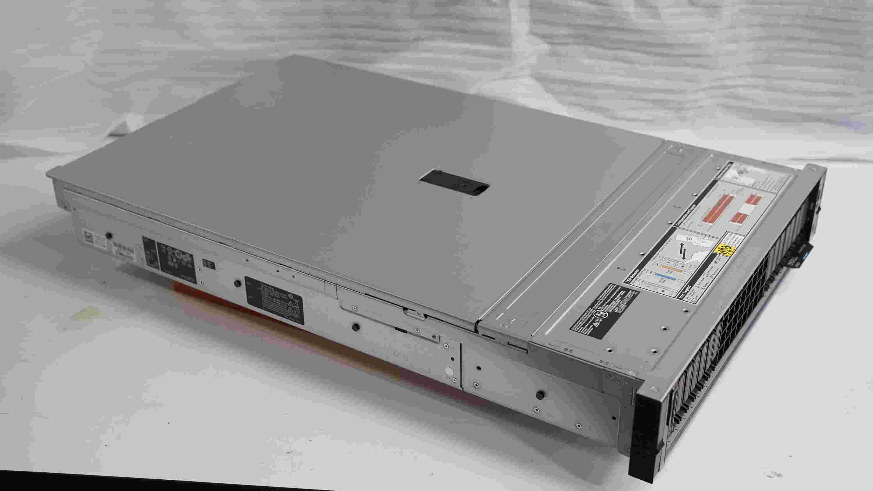
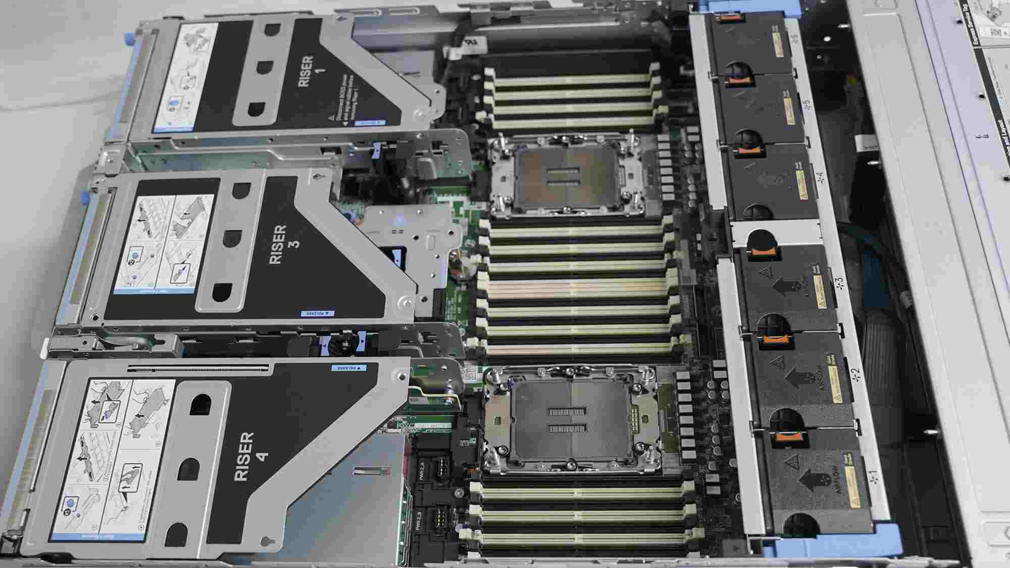
Multi-layer PCBs for high-bandwidth memory (HBM) interfaces and GPU carrier boards used in South San Francisco data centers.
Rigid-flex multi-layer boards for wearable health monitors and surgical robotics developed in the SF Medical District.
Sensor-fusion PCBs for LiDAR and Radar modules, meeting automotive-grade reliability for autonomous vehicle testing in the Bay Area.
Moving toward trace/space widths of 30/30μm to support next-gen chiplets and heterogeneous integration.
Integrating resistors and capacitors directly into the internal layers to reduce the footprint for SF's IoT startups.
Transitioning to halogen-free materials and recyclable substrates to align with California's stringent environmental regulations.

A: Multi-layer boards allow for higher component density and more complex circuitry in a smaller footprint, which is critical for the compact designs of Bay Area startups in medical and wearable technology. They also provide better EMI shielding and signal integrity for high-frequency applications.
A: We implement strict ISO-based quality management systems. Every board undergoes Automated Optical Inspection (AOI), electrical performance testing, and reliability stress testing. For SF-based aerospace or medical clients, we provide full traceability and compliance documentation.
A: Yes! We specialize in quick-turn prototypes with 24-48 hour lead times for standard multi-layer stacks, allowing SF engineers to iterate quickly during the R&D phase before moving to full-scale production.
A: Absolutely. Our R&D team of 60-300 engineers works closely with clients to optimize signal integrity, dielectric constant (Dk) requirements, and thermal dissipation through custom material selection and stack-up engineering.
A: All our products are RoHS and REACH compliant. We also offer halogen-free material options to meet the environmental sustainability goals of San Francisco’s green-tech initiatives.

As a global leader in Multi-layer Circuit Board manufacturing, VoltDRAM Semiconductor Co., Ltd. is committed to empowering the next generation of computing. Whether you are a system integrator in San Francisco or a data center operator in Silicon Valley, our stable, fast, and efficient memory and PCB products provide the foundation for your success. With over 1,500 supply chain partners and a decade of industry expertise, we are your trusted partner in high-performance hardware.