Greater Jakarta, including the industrial hubs of Bekasi, Cikarang, Karawang, and Tangerang, has rapidly emerged as a critical manufacturing powerhouse within Southeast Asia. Driving this momentum is a dramatic shift toward advanced automotive electronics, industrial automation, localized consumer electronics, and high-performance telecommunication modules. As manufacturing centers migrate toward complex printed circuit board assemblies (PCBAs), the demand for high-reliability Surface Mount Technology (SMT) laser stencils has surged.
However, local production lines face distinct geographical challenges. The tropical humidity levels characteristic of the Jabodetabek region significantly affect solder paste rheology. High moisture content can lead to paste slumping, bridging, or insufficient release during printing cycles. Resolving these challenges requires stencil technology with ultra-smooth aperture sidewalls, optimized area ratios, and advanced nano-coating finishes that repel flux. Partnering with a world-class stencil exporter ensures that Jakarta SMT lines achieve higher yields, minimal rework, and maximum throughput.
Ambient humidity levels in Indonesian manufacturing zones often fluctuate, causing variations in solder paste viscosity. A high-grade laser-cut stencil provides the necessary compensation by using precise aperture sizing to prevent bridges.
Maintaining an Area Ratio above 0.66 is critical for fine-pitch components (such as 0.3mm BGA or 0201 packages) to ensure reliable paste transfer. We calculate and inspect every aperture design prior to production.
We use high-tensile, fine-grain SUS304 stainless steel foils. This material provides superior dimensional stability and edge definition, reducing stencil distortion under repeated squeegee pressure.
Our state-of-the-art fiber laser cutting systems achieve cutting spot diameters down to 20μm, ensuring burr-free aperture walls with taper angles designed to facilitate effortless solder paste release.
Optional fluxophobic nano-coating creates an ultra-thin barrier on the bottom surface, reducing cleaning frequency from once every 3 print cycles to once every 10-15 cycles, enhancing overall SMT efficiency.
| Stencil Parameter | Standard Specification | Advanced Option (Fine-Pitch) | Application Target |
|---|---|---|---|
| Foil Thickness | 0.10mm - 0.15mm (±3μm) | 0.08mm - 0.18mm (±2μm) | 0402/0201 Components, QFN/BGA Packages |
| Aperture Taper | 1° to 1.5° (Trapezoidal) | Optimized 1.8° - 2.2° | Improves Paste Release in High-Humidity SMT Rooms |
| Positional Accuracy | ±10μm across 600mm | ±5μm across 600mm | High-Density Double-Sided PCBA Alignment |
| Cutting Speed & Quality | Standard Fiber Cut | Electropolished & Nano-Coated | Ultra-Low Defect Rate (DPMO) for Smart Devices |
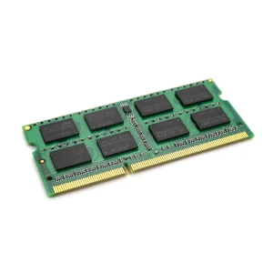
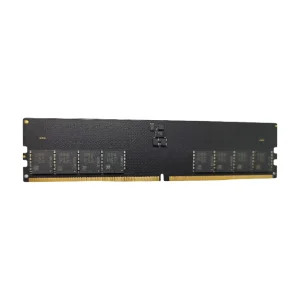
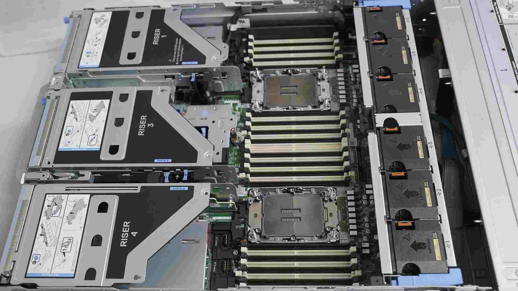
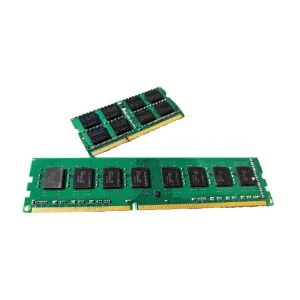
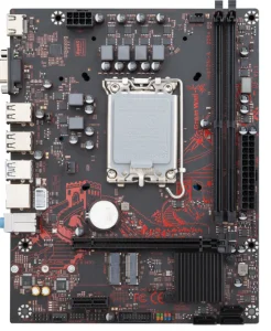
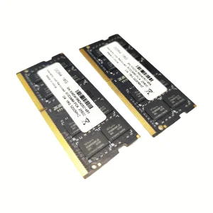
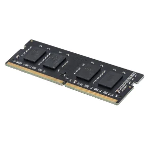
As a global semiconductor provider, VoltDRAM Semiconductor Co., Ltd. is at the forefront of memory design and hardware production. Our state-of-the-art facilities, ranging from 320–480㎡, feature advanced micro-assembly and automated inspection lines that handle everything from DDR5 high-speed memory modules to multi-layer server motherboards.
With 6 to 9 years of export experience and a deep bench of 60 to 300 R&D engineers, we ensure our global partners receive component batches optimized for advanced SMT assembly. Our SMT stencils are engineered using China's Industry 4.0 supply chain capabilities, enabling us to deliver micron-level precision and rapid order fulfillment.
Years Export Experience
Annual Export Value
Expert R&D Engineers
Supply Chain Partners
Our QC processes integrate automated optical inspection (AOI) with precise physical tension measurements. We utilize specialized optical systems to verify that stencil apertures remain completely free of microscopic burrs.


Automotive components demand zero-defect performance. Our step stencils provide localized thickness control, ensuring correct solder volume for both high-power components and fine-pitch sensor controllers.
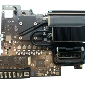
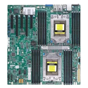
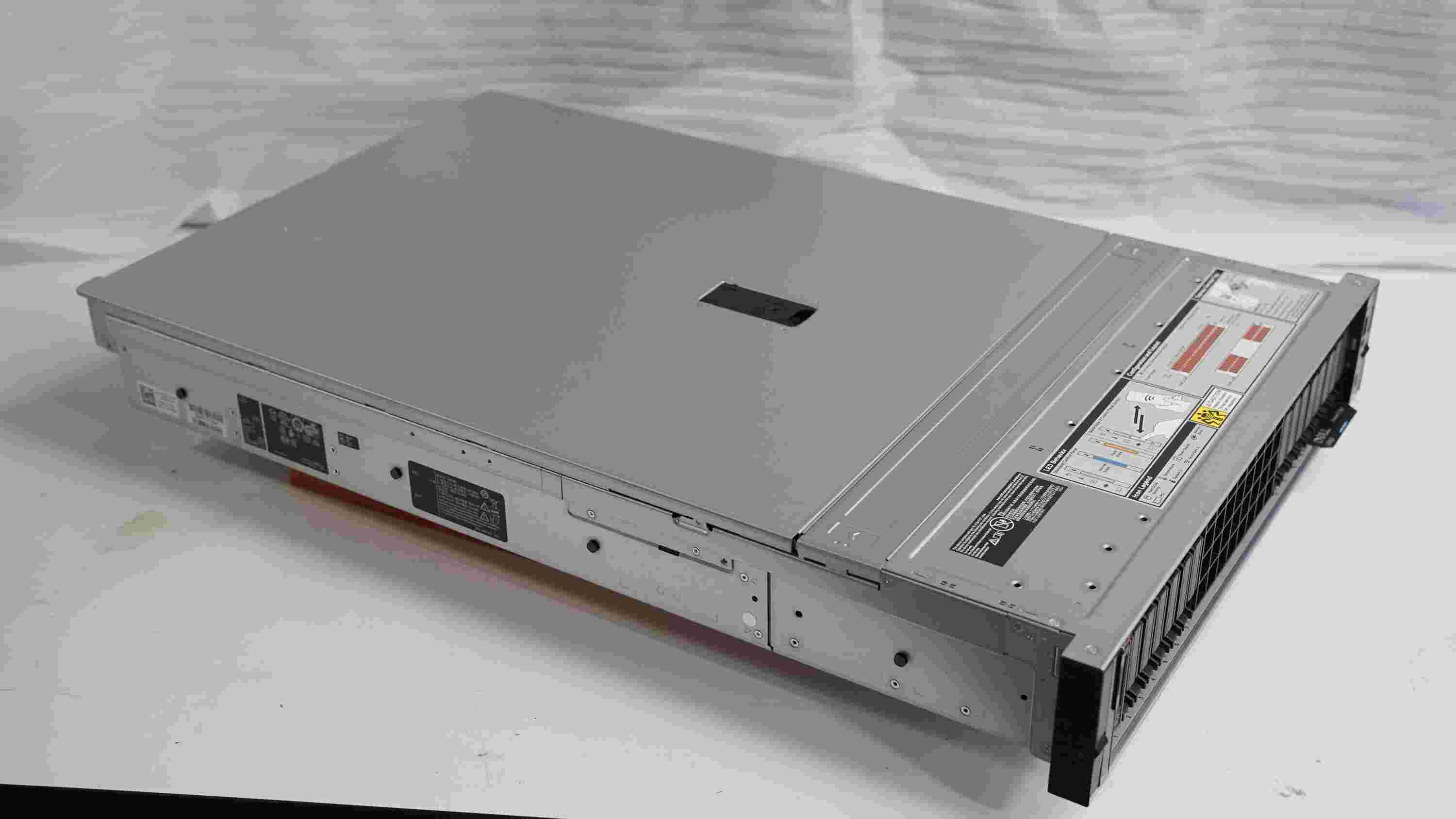
Server motherboards require thousands of solder joints on thick multilayers. Our custom stencils are engineered to maintain high print speeds without clogging, preventing voids in critical ground pads.
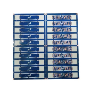
For micro-BGAs and 01005 passives in small wearables, we supply electropolished foils that ensure excellent paste release, lowering defect rates and keeping lines running continuously.
We ensure our operations and materials align with major international frameworks (including RoHS and REACH directives) and meet the performance standards required by industrial facilities across Jakarta, Bekasi, and Cikarang.
To protect stencils during maritime or air transport from China to Jakarta, we use robust packaging that guards against high humidity, temperature swings, and physical impacts. Our technical support team assists you with pre-production CAD verification to ensure proper design layout before fabrication begins.

High ambient humidity causes solder paste to absorb moisture, which lowers its viscosity and can lead to issues like paste slumping or bridging. To counter this, we optimize the stencil's trapezoidal aperture geometry (typically using a 1° to 2° taper) and apply a hydrophobic nano-coating. This combination helps maintain clean paste release even in challenging environmental conditions.
Thickness is determined by balancing the requirements of the smallest components against those of larger, leaded parts. We follow IPC-7525 guidelines, aiming for an Area Ratio of >0.66 and an Aspect Ratio of >1.5. If the layout contains both fine-pitch components (like 0.3mm BGAs) and larger connectors, we recommend a step-up or step-down multi-level stencil to deliver the correct solder volume across all pads.
Electropolishing uses a chemical bath to smooth the micro-burrs left on aperture walls after laser cutting. This process reduces surface roughness, allowing solder paste to slide out more easily during separation and minimizing the buildup of paste residue.
Stencils are cleaned, secured to flat backboards, and vacuum-sealed in anti-static, moisture-barrier bags with desiccants. They are then placed inside padded, impact-resistant shipping crates to prevent bending or loss of tension during transit.