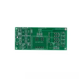
Precision-engineered structural parts matching critical high-density SMT layout requirements.
The electronics manufacturing sector within the Russian Federation is undergoing a monumental shift toward domestic self-reliance, localized production, and high-frequency computing infrastructure. Key industrial zones including the Technopolis Moscow, Zelenograd Microelectronics Cluster, Novosibirsk Academgorodok, and the scientific hubs of St. Petersburg are scaling their Surface Mount Technology (SMT) capacities. As a foundational tool in the SMT assembly line, the Laser Stencil (also known as a laser-cut solder paste stencil or SMT template) governs the precision and yield of component placements. From basic consumer devices to sophisticated industrial motherboards, the quality of the laser stencil determines the presence of assembly defects such as solder bridging, voids, and insufficient wetting.
In Russia, industrial sectors such as telecommunications, domestic server systems (supporting Yandex, Rostelecom, and local cloud nodes), automotive control systems, and defense electronics mandate highly stable PCB configurations. Since SMT lines in regions like Yekaterinburg and Chelyabinsk run high-mix, low-to-medium volume production, stencils must maintain excellent dimensional stability under varying temperature and cleaning cycles. Our SMT Laser Stencils provide localized design adaptions, accommodating unique Russian mechanical printer frameworks and meeting strict national industrial standards.
We utilize state-of-the-art fiber laser cutting machinery running multi-axis motion controls to guarantee sub-micron precision. Each aperture is cut with a trapezoidal profile (tapered walls angled at 1.5 to 2 degrees) to promote flawless solder paste release during the squeegee sweep.
Standard stainless steel foils possess a grain structure size of 15–25 microns, which can cause micro-cracks along cut paths. By contrast, our Fine-Grain (FG) foils feature a grain size of 1–5 microns. This enables extremely smooth laser cuts, minimizing wall roughness to less than 1.5 microns Ra.
Modern high-density PCBA designs are rarely uniform. Power management ICs (PMICs) require high solder volume, whereas small BGA/WLCSP devices demand micro-deposits. To address these competing requirements on a single board, we manufacture multi-level Step-Up & Step-Down Stencils. Using precise chemical milling or CNC laser ablation, specific zones of the metal mask are reduced or increased in thickness.
This technology is widely utilized by Russian telecommunication hardware designers to integrate RF shields with micro-processors on the same assembly run.
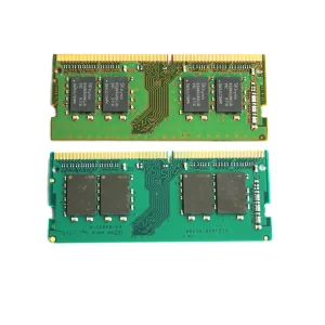
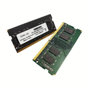
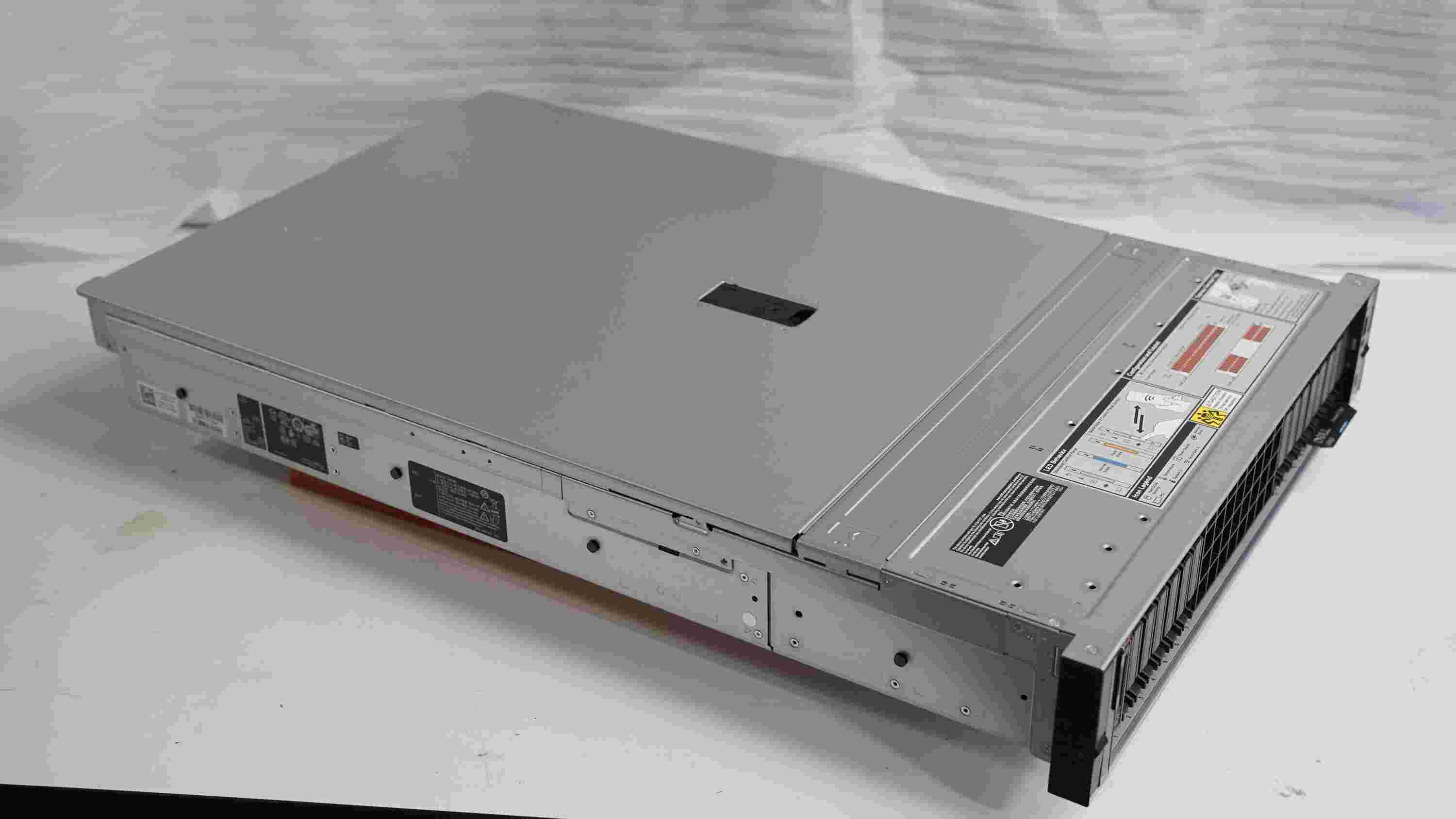
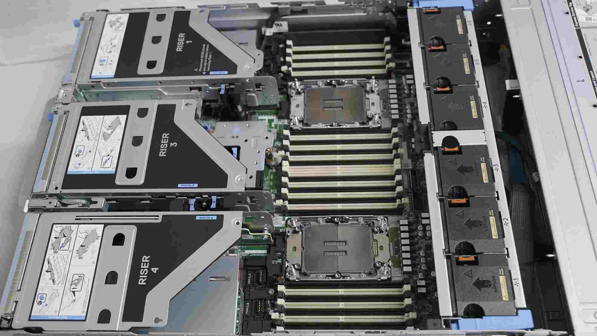
VoltDRAM Semiconductor Co., Ltd. is a professional DDR5 memory manufacturer specializing in high-performance DRAM solutions for servers, PCs, and data center applications. The company was registered between 2015–2018 and has rapidly developed into a reliable global supplier in the memory industry. Our manufacturing facility covers an area of approximately 320–480㎡, equipped with advanced production and testing lines. We generate an annual export revenue of around USD 8–18 million, with 6–9 years of export experience and 8–15 years of industry expertise in semiconductor memory development and manufacturing.
Quality is at the core of VoltDRAM. We implement strict ISO-based quality management systems, combined with automated optical inspection (AOI), electrical performance testing, burn-in testing, and reliability stress testing to ensure stable product performance. Our quality control team consists of 35–80 experienced inspectors, ensuring every batch meets international standards.
With a strong international trade background, VoltDRAM mainly serves markets in North America, Europe, Southeast Asia, and the Middle East. We maintain long-term cooperation with over 600–1,500 supply chain partners, supporting a stable and efficient production ecosystem.
Our customers include OEM/ODM brands, system integrators, data center operators, and industrial computer manufacturers. We have strong R&D capabilities focused on high-speed DDR5 architecture optimization, signal integrity improvement, and power efficiency design. We also provide full customization options, including PCB design, memory capacity configuration, frequency tuning, and branding solutions. Each year, we launch approximately 120–450 new product variants, supported by a dedicated R&D team of 60–300 engineers. Our innovation-driven approach allows us to continuously deliver competitive and high-performance memory solutions to global customers.


Procuring high-tech industrial parts from abroad demands robust logistics pipelines. For Russian enterprises based in Moscow, St. Petersburg, Perm, or Vladivostok, transit time, Customs clearing, and certification conformity are key metrics. We streamline the delivery of Laser Stencils and electronic assemblies with dedicated transportation corridors, optimizing both cost and safety.
Recognizing the urgency of SMT assembly timelines, we deploy Express Air Freight options to Moscow Sheremetyevo (SVO) and Domodedovo (DME) airports, yielding arrival times of 3–5 working days. For bulk structures and framed stencils, cost-effective Rail Transport via the New Silk Road network ensures reliable, temperature-stable delivery across the Urals to terminal nodes in Russia.
All imported equipment and sub-assemblies undergo strict scrutiny at the Eurasian Economic Union (EAEU) border. We provide clear, pre-inspected customs documentation, HS Code declarations (typically under heading 8442 for printing plates/cylinders), and EAC declarations of conformity to ensure delay-free clearance.
As Russia's localized semiconductor and PCBA industries approach higher levels of integration, conventional stencil-cutting technologies will face limits. Our technical roadmap focuses on deploying active solutions to resolve stencil manufacturing issues before they reach the production floor.
We answer the most common engineering and commercial questions regarding stencil selection, material performance, and supply logistics for Russian enterprises.
Broad spectrum electronic components and modular boards optimized for high-reliability systems.